Blog
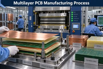
Multilayer PCB Manufacturing Process: Registration, Lamination and Testing
See how multilayer PCBs are fabricated from stack-up and inner layers through lamination, drilling, plating, inspection and electrical testing.



See how multilayer PCBs are fabricated from stack-up and inner layers through lamination, drilling, plating, inspection and electrical testing.
If you have any enquiry about quotation or cooperation, please feel free to email us at [email protected] or use the following enquiry form. Oursales representative will contact you within 24 hours. Thank you for your interest in our products.