Blog
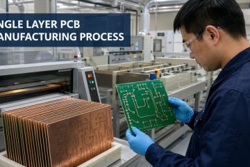
Single Layer PCB Manufacturing Process: Imaging, Etching and Quality Checks
Follow the single layer PCB manufacturing process from DFM and copper imaging through etching, drilling, solder mask, finish and electrical testing.



Follow the single layer PCB manufacturing process from DFM and copper imaging through etching, drilling, solder mask, finish and electrical testing.
If you have any enquiry about quotation or cooperation, please feel free to email us at [email protected] or use the following enquiry form. Oursales representative will contact you within 24 hours. Thank you for your interest in our products.