Blog
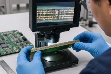
How to Identify PCB Layers: Visual Clues, Files and Limits
Learn how to identify PCB copper layers using design files, board-edge clues, vias, X-ray, and cross-section evidence, with clear limits for each method.



Learn how to identify PCB copper layers using design files, board-edge clues, vias, X-ray, and cross-section evidence, with clear limits for each method.
If you have any enquiry about quotation or cooperation, please feel free to email us at [email protected] or use the following enquiry form. Oursales representative will contact you within 24 hours. Thank you for your interest in our products.