




How can you identify how many layers a PCB has?
The most reliable way to identify PCB layer count is to inspect the controlled design or fabrication data and confirm the stackup drawing. If those records are unavailable, use the board edge, via structures, light transmission, X-ray, or a prepared cross-section as evidence—but label the result as an estimate unless the internal copper layers are directly verified. Visible traces on the top and bottom do not reveal every buried plane or signal layer.
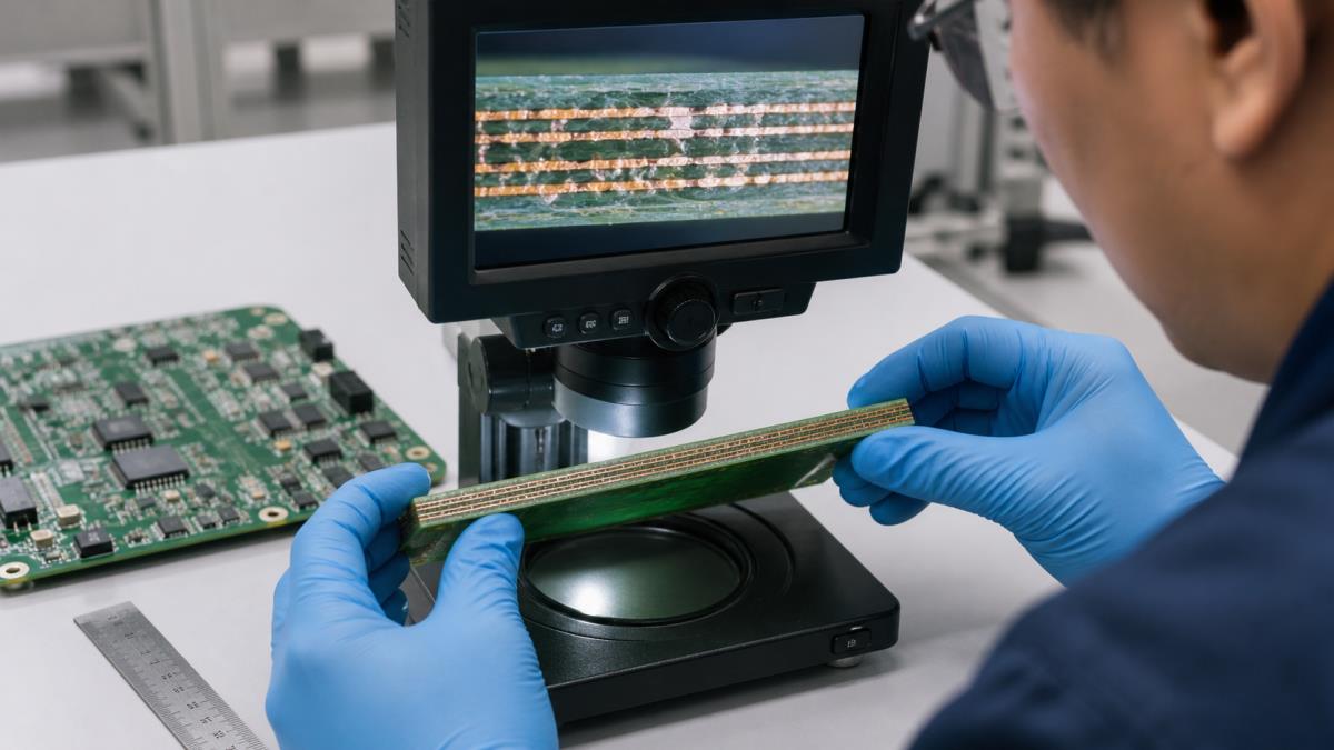
Count copper layers, not every material or CAD layer
When manufacturers call a board 2-layer, 4-layer, or 6-layer, they normally mean conductive copper layers. Solder mask, silkscreen, coverlay, core, and prepreg are physical or documentation layers but are not added to the marketed copper-layer count.
| Layer term | What it does | Counts as a PCB copper layer? |
|---|---|---|
| Top/bottom copper | Routes signals, power, or ground on the outer surfaces | Yes |
| Inner signal or plane copper | Routes internal signals or distributes power/ground | Yes |
| Core and prepreg | Insulate and bond copper layers | No |
| Solder mask | Protects outer copper and defines exposed areas | No |
| Silkscreen/legend | Adds component and assembly markings | No |
| Mechanical or documentation layer | Describes outline, dimensions, notes, or assembly | No |
Start with files and records when they exist
Look for the native PCB design, Gerber or ODB++ package, fabrication drawing, stackup, purchase order, job traveler, impedance report, or supplier certificate of conformance. A stackup drawing should identify each copper layer and the dielectric between layers. Gerber names may help, but do not trust filenames alone: open every file in a viewer and verify whether it contains copper, mask, legend, drill, or mechanical data.
Use an evidence hierarchy instead of one visual trick
| Method | Typical confidence | Main limitation |
|---|---|---|
| Approved stackup plus fabrication data | High | Must match the exact board revision |
| Manufacturer job record | High | Requires traceable supplier and lot information |
| Prepared microsection | High | Destructive to the sampled coupon or board area |
| Suitable X-ray/CT inspection | Medium to high | Resolution, copper overlap, and interpretation matter |
| Clean board-edge microscopy | Medium | Internal copper may not reach the observed edge |
| Via and routing clues | Low to medium | Suggest multilayer construction but rarely prove exact count |
| Flashlight or translucency | Low | Material, thickness, mask, and copper planes obscure the view |
Inspect the board edge carefully
Under oblique light and magnification, a clean routed edge may show alternating dielectric and copper lines. Inspect several edges because an internal copper layer may be pulled back from one edge or contain little copper at that location. Dark resin, glass weave, surface finish, edge plating, burrs, and contamination can hide the stack.
Do not scrape a functional board merely to expose layers. If destructive inspection is acceptable, choose a noncritical coupon or sacrificial board and use a controlled cross-section method.
Understand what vias can and cannot prove
Plated through holes connecting visible copper on both sides are common on both two-layer and multilayer boards. Blind or buried vias strongly indicate a multilayer construction, but a visible blind-via feature still does not automatically reveal the total number of copper layers. Filled or capped vias, via-in-pad, laser microvias, and tented holes may also be hard to classify from the surface.
Use via clues to decide whether further inspection is justified, not to invent an exact stackup.
Use light transmission only as a rough screen
A strong light behind a thin, lightly colored board may reveal broad copper shadows or routing patterns. An opaque plane, thick laminate, dark solder mask, metal core, dense copper, or filled material can block the view. If you see internal patterns, you have evidence of internal copper; if you see nothing, you have not proved that the board has only two layers.
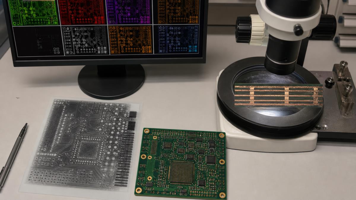
Open Gerber or ODB++ data in a real viewer
Load the complete package and group files by function. Copper files usually contain pads, traces, pours, or planes. Confirm top and bottom copper, then count genuine internal copper layers. Check drill files and the fabrication drawing to understand blind, buried, or through-hole spans. If the names are ambiguous, ask the data owner or fabricator; do not classify a plane drawing or paste layer as copper merely because it looks dense.
Use X-ray when the board must remain intact
X-ray can reveal hidden routing, vias, planes, and layer registration without cutting the board. Standard 2D X-ray may combine multiple copper layers into one projection, so exact counting can remain difficult when copper overlaps. Higher-resolution imaging, angled views, tomography, or CT may separate features more clearly. Ask the inspection provider what resolution and method are needed for the board thickness and feature size.
Use a microsection when the answer must be proven
A metallographic cross-section exposes the laminate structure directly. The sample is cut, mounted, ground, polished, and examined under magnification. A suitable section can show copper layers, dielectric thickness, plated holes, registration, resin condition, and other construction details. Because section location matters, choose a coupon or area that crosses representative copper and relevant vias.
Use a qualified lab when the result supports a supplier dispute, reliability investigation, compliance record, or production acceptance decision.
Follow a non-destructive identification sequence
- Record the board part number, revision, date code, supplier, and assembly identity.
- Search the controlled source package, drawing archive, purchase record, or manufacturer documentation.
- Inspect top and bottom routing, via types, edge connectors, exposed cutouts, and several board edges.
- Use magnification and controlled lighting; take scale-referenced photographs.
- Open any fabrication data in an independent viewer and classify each file by function.
- If uncertainty remains, use X-ray or CT when the board must survive.
- Escalate to a representative microsection only when exact construction evidence is necessary.
- Record the method, observed evidence, confidence level, and remaining uncertainty.
Avoid common layer-count mistakes
- Counting solder mask, silkscreen, or dielectric as conductive layers
- Assuming a through-hole via proves a multilayer board
- Assuming no transmitted light proves a two-layer board
- Counting Gerber files without opening and classifying them
- Using files from a different revision as proof
- Reading one board edge where internal copper is pulled back
- Confusing metal-core construction with an internal copper signal layer
- Claiming an exact count from an unclear 2D X-ray projection
Know when layer count is not enough
For repair, reverse engineering, quoting, or redesign, you may also need layer order, dielectric thickness, copper weight, plane assignments, via spans, impedance structures, material type, surface finish, and controlled-depth features. Two boards with the same layer count can behave very differently. If manufacturing or electrical performance matters, request the complete stackup rather than stopping at “four layers.”
Prepare a useful inspection or supplier request
Provide the board identifier and revision, photographs, dimensions, reason for the investigation, whether destructive analysis is permitted, and the required confidence. Ask the lab or supplier to report method, sample location, copper-layer count, layer order, dielectric measurements where needed, via construction, image scale, and any limitation that prevents a definitive conclusion.
PCB layer identification FAQ
Can you tell PCB layer count by looking at the surface?
You can often distinguish a simple single-sided board and may suspect a multilayer board from vias and routing density, but the surface usually cannot prove the exact internal copper-layer count.
Does every multilayer PCB have an even number of layers?
Many common production stackups use even copper-layer counts for symmetry and process reasons, but do not use that convention as evidence for an unknown board. Verify the actual stackup.
Does a via mean the PCB has four layers?
No. Plated through vias are used on two-layer boards as well. Blind or buried vias indicate internal connections, but do not alone prove the total layer count.
Can a flashlight reveal inner PCB layers?
Sometimes it reveals shadows in thin or sparse boards. Failure to see a pattern is inconclusive because copper planes, material, mask, and thickness can block light.
Can X-ray count PCB layers?
It can provide strong evidence, especially with appropriate angles or tomography, but overlapping copper in a basic 2D projection may prevent an exact count.
What is the most accurate destructive method?
A correctly located, prepared, and interpreted metallographic cross-section can directly show the stack. The method and sample must be suitable for the question.
How do I identify layers in Gerber files?
Open every file in a viewer, distinguish copper from mask, paste, legend, drill, and mechanical data, and confirm the file set against the fabrication drawing.
Are power and ground planes counted as layers?
Yes. A conductive internal plane is a copper layer even if it contains little signal routing.
Is solder mask a PCB layer?
It is a physical coating layer, but it is not included when a PCB is sold as a 2-layer, 4-layer, or 6-layer copper board.
Why must I know the exact PCB revision?
Different revisions can change stackup, routing, via structure, or layer count while keeping a similar outline and component arrangement.
Request stackup and fabrication review
If you need to reproduce, quote, or redesign a board, send the available Gerber data, drawings, board photographs, dimensions, revision information, and required evidence through the PCBTRY contact page. State whether you need a quick layer-count estimate, a manufacturable replacement stackup, or formal construction verification.



0 Comments