Blog
High Frequency PCB Assembly Process: RF Materials, Reflow and Testing
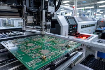
Learn how high-frequency PCB assembly controls materials, solder paste, placement, reflow, cleaning, connectors, inspection and RF acceptance testing.



Learn how high-frequency PCB assembly controls materials, solder paste, placement, reflow, cleaning, connectors, inspection and RF acceptance testing.
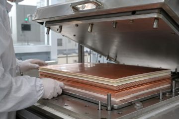
Learn how high-frequency multilayer PCBs are laminated, including material compatibility, surface preparation, registration, press control and post-lamination RF checks.
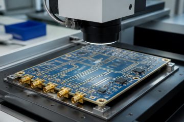
Designing a high frequency PCB is not the same as laying out a standard digital board. Once signals rise above a few hundred MHz, every physical dimension on the board — trace width, dielectric thickness, via geometry, reference plane continuity — starts to affect electrical performance in ways that a Read more
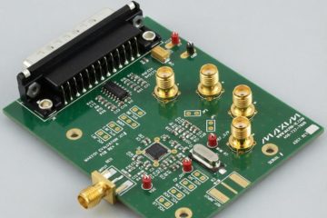
When RF engineers talk about “high frequency PCB,” they’re usually talking about boards that carry signals above 500 MHz — often well into the tens of gigahertz. At those frequencies, every design choice matters: the laminate, the copper surface roughness, the via placement, even the solder mask formulation. A board Read more
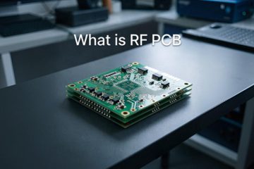
An RF PCB is a printed circuit board built to carry radio-frequency signals with controlled impedance, low loss, stable grounding, and predictable electromagnetic behavior. In RF work, the PCB is not just a carrier for components. The board material, copper geometry, stackup, via transition, solder mask, connector launch, and ground Read more
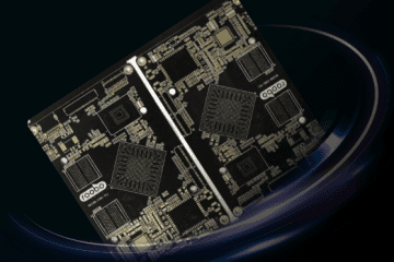
What is an HDI PCB? – The Backbone of Modern Electronic Devices HDI PCBs (High-Density Interconnect Printed Circuit Boards) are among the most critical fundamental components in today’s electronics industry, representing the forefront of printed circuit board technology development. HDI refers to circuit board design and manufacturing technology that utilizes Read more
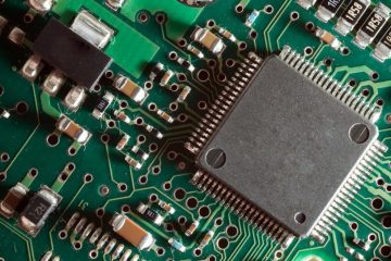
Introduction Whether you’re using a smartphone, operating a computer, or starting your microwave, you are relying on a Printed Circuit Board (PCB). PCBs are hidden inside nearly all electronic devices, serving as their indispensable core skeleton. So, what exactly is the purpose of this “green board” covered in lines and Read more
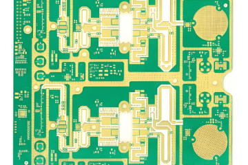
High frequency PCB design is an essential part of modern electronics. Whether you’re designing for 5G communication, satellite systems, or high-speed data processing, understanding the key elements of high frequency PCB design ensures a functional, reliable, and efficient product. Let’s walk through what makes high frequency PCB design unique and Read more
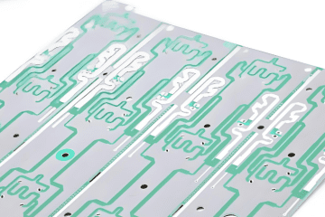
In today’s fast-paced world of electronics, the demand for faster, more reliable communication has never been higher. High frequency PCB (Printed Circuit Board) communication circuits are at the heart of this evolution. From smartphones to satellite communications, these circuits ensure seamless data transmission, making them indispensable in a wide range Read more
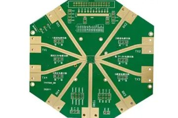
5G technology is defined by its high speed, low latency, and massive capacity—but operating in high-frequency bands like millimeter waves and Sub-6GHz poses unique challenges: signals are prone to attenuation and distortion during transmission. High-frequency/hybrid laminates act as the “signal highways” for 5G base stations and end devices, directly determining Read more
If you have any enquiry about quotation or cooperation, please feel free to email us at [email protected] or use the following enquiry form. Oursales representative will contact you within 24 hours. Thank you for your interest in our products.