




Designing a high frequency PCB is not the same as laying out a standard digital board. Once signals rise above a few hundred MHz, every physical dimension on the board — trace width, dielectric thickness, via geometry, reference plane continuity — starts to affect electrical performance in ways that a typical ERC/DRC check will never catch.
At 28 GHz, a 0.5 mil deviation in trace width can shift characteristic impedance by 2-3 ohms. A via stub of just 10 mils can add measurable return loss at millimeter-wave frequencies. These are not theoretical concerns — they are the daily reality of RF and microwave PCB design.
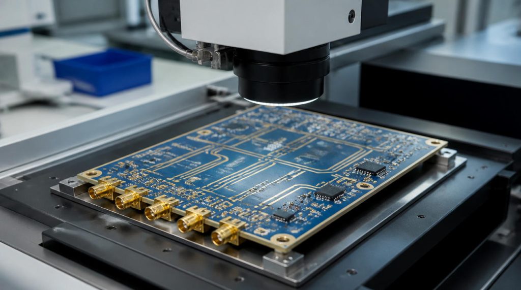
This guide walks through the specific design rules, stackup strategies, impedance control methods, trace routing guidelines, via design techniques, and EMI suppression strategies that engineers need when designing high frequency PCBs. Each section covers what to do, why it matters, and what happens if you skip it.
For a broader overview of high frequency PCB materials, construction methods, and applications, see our complete high frequency PCB guide.
Start With the Stackup — It Shapes Everything
The PCB stackup is the single most important design decision in any high frequency board. It determines the impedance environment, defines which layers can carry RF signals, constrains your routing options, and directly influences both performance and manufacturing cost.
Most design mistakes at high frequency trace back to a stackup that was chosen too late or not chosen deliberately at all.
Why the Stackup Comes Before Layout
In a standard digital PCB, you can often choose a stackup after the schematic is complete. In high frequency design, the stackup must be defined before any RF routing begins. Here’s why:
- Impedance depends on stackup geometry. Every impedance calculation uses trace width, dielectric thickness, and Dk — all of which are stackup parameters. You cannot set a trace width target without knowing the layer structure.
- Return current paths are fixed by the stackup. High frequency signals require a continuous reference plane directly adjacent to every signal layer. If the stackup doesn’t place one there, no amount of routing cleverness can fix it.
- Material choices are locked in the stackup. Once you commit to a 6-layer structure with specific laminates and prepregs, changing a material requires a full redesign — not just a BOM update.
- Manufacturing feasibility depends on the stackup. Layer count, material mix, copper balance, and via structure all affect yield. A stackup that looks right on paper may be impossible or extremely expensive to build.
Questions to Answer Before Designing Your Stackup
Before drawing a single trace, work through these questions:
| Question | Why It Matters |
|---|---|
| What is the highest operating frequency? | Determines the minimum Dk stability and Df requirements. Above 10 GHz, standard FR4 is no longer viable for RF layers. |
| How many RF signal layers are needed? | Each RF layer needs its own reference plane. More RF layers = more layers total = higher cost. |
| Are there differential pairs? | Differential pairs require precise spacing and matched impedance. The stackup must support the target impedance and coupling. |
| Are there high-speed digital signals on the same board? | Mixed-signal designs need clear separation between RF and digital sections. Consider a hybrid stackup with different materials on different layers. |
| What is the power dissipation of active components? | High-power RF amplifiers need thermal vias, thicker copper, or metal-core layers. The stackup must accommodate thermal paths. |
| What impedance tolerance is required? | Tighter tolerance (±3% or ±5%) requires tighter stackup control and more expensive materials. ±10% is standard for most RF work. |
Reference Plane Placement Rules
These are non-negotiable rules for any high frequency stackup:
- Every RF signal layer must be immediately adjacent to a complete, unbroken ground plane. This is the #1 rule. If your RF trace is on Layer 1, Layer 2 must be a solid ground plane with no gaps, no splits, and no copper pours that create slots.
- Never route an RF signal layer next to a power plane. Power planes are noisy and provide poor high-frequency return paths due to their impedance and connection to decoupling networks.
- Avoid placing two RF signal layers back-to-back (Layer 1 and Layer 2 both carrying RF signals). Without a ground plane between them, the signals will couple strongly and create uncontrolled crosstalk.
- Keep ground planes away from the board edges where possible. Edge effects can cause field radiation and impedance discontinuities at very high frequencies.
Hybrid Stackup Design Strategy
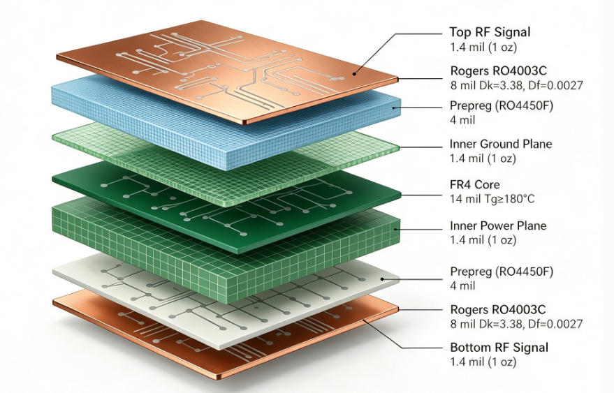
For most high frequency designs, a hybrid stackup is the most practical and cost-effective approach: use high-performance laminates (like Rogers RO4003C or RO4350B) for the RF signal layers, and standard FR4 for the inner ground and power planes.
This works because:
- The RF signal energy is concentrated in and near the RF laminate layer (the electromagnetic field doesn’t extend deeply into the ground plane below).
- FR4 ground and power planes provide adequate performance at any frequency — they don’t carry signals that need controlled impedance.
- FR4 is 3-5x cheaper than Rogers materials, so limiting the high-performance material to just 1-2 layers saves significant cost.
Important: When building a hybrid stackup, use a prepreg that is compatible with both materials. Rogers RO4450F is designed as a bonding layer for RO4003C and RO4350B — it provides reliable adhesion and controlled Dk at the interface. Standard FR4 prepreg can also work, but verify the adhesion and CTE compatibility with your fabricator.
Stackup Examples for Common Applications
4-Layer Stackup — Simple RF Module
| Layer | Function | Material | Thickness |
|---|---|---|---|
| L1 (Top) | RF signal | Rogers RO4003C | 8 mil (0.2 mm) |
| Prepreg | Bonding | RO4450F | 4 mil (0.1 mm) |
| L2 | Ground plane | FR4 | 14 mil (0.35 mm) |
| L3 | Power / digital | FR4 | 14 mil (0.35 mm) |
| Prepreg | Bonding | RO4450F | 4 mil (0.1 mm) |
| L4 (Bottom) | RF signal | Rogers RO4003C | 8 mil (0.2 mm) |
6-Layer Stackup — 5G Base Station RF Board
| Layer | Function | Material | Thickness |
|---|---|---|---|
| L1 | RF signal | Rogers RO4350B | 10 mil |
| Prepreg | Bonding | RO4450F | 5 mil |
| L2 | Ground plane | FR4 | 12 mil |
| L3 | Digital / control signals | FR4 | 12 mil |
| Core | Core | FR4 | 28 mil |
| L4 | Ground plane | FR4 | 12 mil |
| Prepreg | Bonding | RO4450F | 5 mil |
| L5 | Ground plane | FR4 | 12 mil |
| L6 | RF signal | Rogers RO4350B | 10 mil |
8-Layer Stackup — Complex Multi-Function System
| Layer | Function | Material | Thickness |
|---|---|---|---|
| L1 | RF signal (control) | Rogers RO4350B | 8 mil |
| Prepreg | Bonding | RO4450F | 4 mil |
| L2 | Ground plane | FR4 | 10 mil |
| L3 | Digital signals | FR4 | 10 mil |
| Core | Core | FR4 | 20 mil |
| L4 | Ground plane | FR4 | 10 mil |
| L5 | Power plane | FR4 | 10 mil |
| Core | Core | FR4 | 20 mil |
| L6 | Ground plane | FR4 | 10 mil |
| L7 | Ground plane | FR4 | 10 mil |
| Prepreg | Bonding | RO4450F | 4 mil |
| L8 | RF signal (high-power) | Rogers RO4350B | 20 mil |
For more information on material properties used in these stackups, see our high frequency PCB materials guide.
Impedance Control — From Calculation to Manufacturing
Controlled impedance is the foundation of high frequency signal integrity. Every RF trace on your board acts as a transmission line, and any deviation from the target impedance causes reflection, loss, and distortion. This section covers the models, calculations, tolerances, and practical methods for achieving controlled impedance in high frequency PCBs.
Understanding the Three Impedance Models
The most common transmission line structures used in PCB design are:
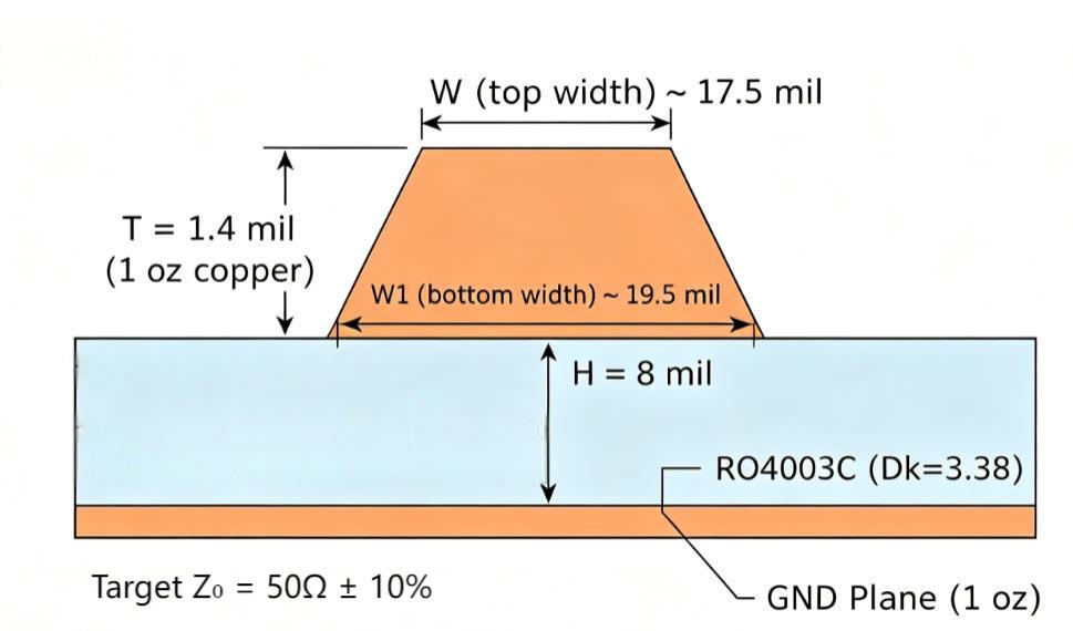
Microstrip: A trace on an outer layer, referenced to a ground plane on the adjacent inner layer. The signal propagates partly through the dielectric and partly through air. This is the most common structure for RF traces and is easier to manufacture.
Stripline: A trace buried between two ground planes (on an inner layer). The signal propagates entirely through the dielectric. Stripline provides better EMI shielding and more consistent Dk, but requires more layers and is harder to route.
Coplanar Waveguide (CPW): A trace on an outer or inner layer with ground copper on the same layer, flanking the trace on both sides. CPW provides additional control over impedance and is useful at very high frequencies (above 30 GHz) where microstrip becomes difficult to control.
Each model has different impedance characteristics. Microstrip is the simplest to design and manufacture; stripline offers better shielding; CPW provides the tightest impedance control at millimeter-wave frequencies. The choice depends on your frequency, layer count, and routing complexity.
Parameters That Affect Impedance
The characteristic impedance of a PCB transmission line depends on these physical parameters:
| Parameter | Symbol | Effect on Impedance |
|---|---|---|
| Trace width | w | Wider trace → lower impedance. A 1 mil change in width can shift impedance by 1-2 ohms at typical RF stackups. |
| Dielectric thickness (to reference plane) | h | Thicker dielectric → higher impedance. This is usually fixed by the stackup and cannot be changed during layout. |
| Copper thickness | t | Thicker copper → slightly lower impedance. 1 oz copper (1.4 mil) vs 0.5 oz copper (0.7 mil) can cause a 1-2 ohm difference. |
| Dielectric constant (Dk) | εr | Higher Dk → lower impedance. Dk also varies with frequency — verify the Dk at your operating frequency, not just the datasheet value. |
| Etch factor (trace cross-section) | — | Copper etching produces a trapezoidal cross-section, not rectangular. This effectively increases the impedance compared to a rectangular trace. Factor this into your calculations. |
Impedance Calculation Methods
Simple formulas exist for microstrip and stripline impedance. The classic microstrip approximation is:
$$Z_0 \approx \frac{87}{\sqrt{\varepsilon_r + 1.41}} \ln\left(\frac{5.98h}{0.8w + t}\right)$$
where:
- $Z_0$ = characteristic impedance (ohms)
- $\varepsilon_r$ = effective dielectric constant
- $h$ = dielectric thickness (mils)
- $w$ = trace width (mils)
- $t$ = copper thickness (mils)
However, do not rely on simplified formulas for production design. They ignore fringing fields, frequency dependence of Dk, trace corner effects, and manufacturing variations. For any board going into production, use a professional impedance calculator such as:
- Polar Si9000 — the industry standard for PCB impedance calculation. Used by virtually all PCB fabricators.
- Altium Designer’s Layer Stack Manager — integrated impedance calculator for designers working in Altium.
- Keysight ADS / Ansys HFSS — for full-wave 3D electromagnetic simulation at frequencies above 30 GHz or for complex geometries.
When you provide impedance targets to your PCB fabricator, they will use their own Polar Si9000 (or equivalent) to verify that the target is achievable with their process and materials. This is standard practice and should be part of every high frequency design workflow.
Setting Impedance Tolerance
The impedance tolerance you specify directly affects both performance and cost:
| Tolerance | Typical Application | Cost Impact |
|---|---|---|
| ±10% | General RF applications below 6 GHz | Standard cost |
| ±5% | Precision RF, 5G, radar, test equipment | 5-15% cost increase |
| ±3% | Millimeter-wave, automotive radar (77 GHz), high-precision instruments | 15-30% cost increase |
Practical advice: Start with ±10% for your first prototypes, verify performance, and tighten the tolerance only if measurements show it’s necessary. Tighter tolerance means tighter process control — narrower lamination thickness windows, more precise etching, and potentially more scrap. Every percentage point of tightening adds cost.
Differential Pair Impedance
If your design includes differential pairs (common in high-speed digital interfaces running alongside RF sections), the differential impedance is controlled by the same stackup parameters plus the spacing between the two traces.
Key points:
- The spacing between differential traces controls the coupling. Closer spacing = more coupling = lower differential impedance for the same single-ended impedance.
- Differential pairs must maintain consistent spacing throughout the route. Any variation in spacing changes the differential impedance and causes reflection.
- Length matching within the pair is critical. Any length skew between the two traces causes mode conversion (differential-to-common), which increases EMI and degrades signal quality.
- Common differential impedance targets are 90Ω (USB, Ethernet) and 100Ω (LVDS, PCIe). For RF differential pairs, 100Ω is the most common target.
Common Impedance Problems
| Problem | Cause | How to Fix It |
|---|---|---|
| Impedance varies along the trace | Trace width changes (e.g., tapering at pads or junctions) | Maintain constant trace width. Use back-taper transitions if width change is unavoidable. |
| Impedance discontinuity at via | Via barrel creates a capacitive discontinuity | Minimize vias in RF paths. Add antipad clearance. At mm-wave, use back-drilling to remove stubs. |
| Impedance shift at reference plane gap | Ground plane has a cut-out or slot under the trace | Never route an RF trace over a gap in the reference plane. Verify ground plane continuity in your layout review. |
| Impedance doesn’t match simulation | Copper surface roughness, etch trapezoid, or Dk variation | Request a cross-section measurement from the fab. Use low-profile copper for tight impedance control at high frequencies. |
RF Trace Routing Rules
Trace routing in high frequency PCBs follows different rules than digital board layout. Every geometric feature of the trace — length, width, bend angle, proximity to other traces, and path over the reference plane — directly affects signal integrity. This section provides the specific rules that RF layout engineers need to follow.
Rule 1: Keep RF Traces Short and Direct
Every millimeter of RF trace adds insertion loss. At 28 GHz, a typical microstrip trace on RO4003C loses approximately 0.3-0.5 dB per inch. That means a 2-inch trace adds 0.6-1.0 dB of loss — which is significant in a system with a tight link budget.
Guideline: Route RF traces as short and straight as possible. If you find yourself adding meanders or detours to meet a length target, re-evaluate the component placement first. The best RF routing starts with the right placement.
Rule 2: Never Use 90° Bends
A sharp 90° corner in a trace creates a localized capacitance increase (the corner acts like a small pad), which causes an impedance dip and signal reflection. At low frequencies, this effect is negligible. At frequencies above 1 GHz, it becomes measurable.
Guideline:
- Use 45° miters for all bends (the standard approach).
- Use curved bends (arc routing) for frequencies above 10 GHz — they provide the smoothest impedance transition.
- Avoid any trace geometry that creates an abrupt width change at a corner.
Rule 3: Maintain Consistent Trace Width
Impedance is directly proportional to trace width. If the width changes — due to poor CAD settings, manual editing errors, or trace tapering at component pads — the impedance changes with it.
Guideline:
- Set a minimum and maximum trace width in your DRC rules and enforce them strictly.
- Avoid auto-router-generated traces that may vary width to fit between obstacles.
- At transitions (e.g., from a 50Ω microstrip to a component pad that’s wider), use a controlled taper rather than an abrupt step.
Rule 4: Separate RF and Digital Traces
Digital signals generate wideband noise that can couple into RF traces through capacitive or inductive coupling. This coupling degrades the signal-to-noise ratio of the RF signal and can cause spurious responses in sensitive receivers.
Guideline:
- Maintain a minimum separation of at least 3× the dielectric thickness between RF traces and any digital trace. For a 10 mil dielectric, that means 30 mil minimum spacing.
- Route RF and digital signals on different layers when possible, with a ground plane between them.
- If RF and digital traces must cross, they should cross at 90° to minimize coupling length.
- Use ground guard traces (grounded copper strips) alongside sensitive RF traces in areas where separation is limited.
Rule 5: Length Matching for Critical Signals
For differential pairs, both traces must be the same length to within the tolerance specified by the interface standard (typically ±5 mils for high-speed digital, ±2 mils for RF differential pairs).
For phased arrays or multi-channel RF systems, traces between channels must be length-matched to maintain phase coherence. The required tolerance depends on the frequency — at 28 GHz, a 1-mil length difference corresponds to approximately 0.2° of phase shift.
Guideline:
- Add serpentine meanders to the shorter trace in a pair to match lengths.
- Place meanders near the driver, not the receiver, to minimize the impact on signal quality.
- Use your PCB tool’s length matching DRC to verify tolerance compliance across all matched groups.
Rule 6: Watch What’s Under the Trace
The reference plane directly beneath an RF trace defines the return current path. If the reference plane has a gap, slot, or split under the trace, the return current must detour around it, creating a loop antenna that radiates and degrades signal integrity.
Guideline:
- Before finalizing layout, run a “return path” visual check: for every RF trace, verify that the reference plane below it is solid and unbroken.
- If a signal transitions between layers (via from L1 to L4, for example), the reference plane at L1 and the reference plane at L4 must be the same net (ground), or you must add stitching vias at the transition point.
- Avoid routing RF traces near board edges or near large cutouts in the ground plane.
Via Design for High Frequency PCBs
Vias are the most underappreciated source of signal degradation in high frequency PCB design. At low frequencies, a via is just a connection between layers. At high frequencies, it becomes a complex three-dimensional structure with parasitic capacitance, parasitic inductance, a resonant frequency, and — if not properly designed — a source of significant signal loss.
The Electrical Model of a Via
At high frequencies, a via can be modeled as:
- A capacitive discontinuity — the via barrel (cylinder of copper) forms a capacitor with the surrounding ground planes. The antipad clearance (the hole in the ground plane around the via) partially compensates, but a net capacitive effect usually remains.
- An inductive element — the current flowing through the via barrel creates a magnetic field, adding inductance. The longer the via, the higher the inductance.
- A resonant structure — at frequencies where the via length approaches a quarter wavelength, the via can resonate, causing a sharp spike in insertion loss. This is why via stubs are so dangerous at high frequencies.
Rule 1: Minimize Vias in RF Signal Paths
Every via in an RF signal path adds loss and potential reflection. The most reliable RF traces are those that stay on a single layer and never transition through a via.
Guideline:
- If possible, route all RF signals on the top layer (Layer 1) to avoid any layer transitions.
- If a layer transition is unavoidable, minimize the number of vias and ensure the transition is designed correctly (see rules below).
- For frequencies above 20 GHz, consider whether the performance impact of a via transition is acceptable for your system. Full-wave EM simulation is strongly recommended.
Rule 2: Control Via Barrel and Antipad Dimensions
The via barrel diameter and the antipad clearance (the unetched area around the via in the reference plane) both affect the parasitic capacitance and the impedance of the via.
Guideline:
- Use the smallest via diameter that your manufacturer can reliably plate. Smaller via barrel = less parasitic capacitance = less impedance discontinuity.
- Increase the antipad clearance to reduce the capacitive coupling between the via and the ground plane. A larger antipad reduces the parasitic capacitance but also reduces the reference plane coverage.
- At frequencies above 10 GHz, work with your PCB fabricator to optimize the via geometry — many manufacturers have standard high-frequency via designs that they’ve validated through EM simulation.
Rule 3: Back-Drill Via Stubs
A via stub is the unused portion of a via barrel — the part that extends beyond the signal layer. For example, if a signal transitions from Layer 1 to Layer 4 through a via, the portion of the via barrel that extends from Layer 4 to the bottom layer is a stub.
At high frequencies, this stub acts as a resonant transmission line. At the frequency where the stub length equals a quarter wavelength, the stub creates a sharp notch in the frequency response — a resonance that can completely kill your signal at that frequency.
Back-drilling (also called controlled-depth drilling) removes the stub by drilling from the opposite side of the board to a controlled depth, eliminating the unused portion of the via barrel.
Guideline:
- For any RF via that transitions more than 2 layers, specify back-drilling in your fabrication notes.
- Back-drilling is a standard process at most experienced RF PCB fabricators. There is usually a small additional cost (typically $50-150 per board, depending on the number of back-drilled vias).
- At millimeter-wave frequencies (above 30 GHz), even a short stub can be problematic. Consider blind vias as an alternative to back-drilling.
Rule 4: Blind and Buried Vias for HDI Designs
For high-density designs where multiple RF signals need to transition between layers in a small area, blind vias (connecting only the outer layer to an inner layer) and buried vias (connecting only inner layers) eliminate the stub problem entirely — there is no unused barrel portion.
Guideline:
- Blind vias are practical for layers 1-to-2 or bottom-to-last-layer transitions. The depth ratio must be achievable by the manufacturer (typical maximum aspect ratio is 1:1 for laser-drilled microvias).
- Buried vias add manufacturing complexity and cost — they require sequential lamination (multiple press cycles). Evaluate whether the performance benefit justifies the cost.
- At frequencies above 40 GHz, microvias (laser-drilled blind vias with diameters of 3-5 mils) are often preferred because their small size minimizes parasitic effects.
Grounding and Shielding Strategies
Proper grounding is essential for high frequency PCB performance. A poorly grounded board can have excellent layout and stackup design but still fail EMI testing or exhibit unexpected resonance. Grounding affects signal integrity, EMI performance, and thermal management simultaneously.
Maintain Continuous Ground Planes
The single most important grounding rule: keep your ground planes solid and unbroken beneath every RF trace.
A continuous ground plane provides:
- A low-impedance return current path that mirrors the signal trace above it.
- Shielding between layers, reducing coupling between RF and digital signals on different layers.
- A stable reference for impedance calculations — gaps or slots in the ground plane change the effective dielectric environment and shift impedance.
Guideline:
- Never route signals (RF or digital) over a gap in the ground plane. If a trace must cross a ground plane boundary, add stitching vias at the crossing point to provide an alternative return path.
- If your design requires splits in the ground plane (e.g., to separate analog and digital ground), ensure that no RF trace crosses the split.
- During layout review, use your PCB tool’s ground plane visualization feature to inspect every layer for gaps, slots, or unexpected copper shapes.
Ground Stitching Vias
Ground stitching vias connect ground planes on different layers, providing a low-impedance vertical connection. They serve three purposes in high frequency design:
- Reduce ground plane impedance — stitching vias in parallel reduce the effective inductance between ground planes, which improves EMI performance.
- Provide return current paths at layer transitions — when a signal transitions from one layer to another via a signal via, a nearby stitching via provides the return current path between the reference planes.
- Form RF fences for shielding — a row of stitching vias placed along an RF trace creates a “via fence” that acts as a waveguide wall, confining the electromagnetic field and reducing radiation and coupling to adjacent traces.
Guideline:
- Place stitching vias within λ/20 (one-twentieth of a wavelength) of each other along RF trace edges. At 10 GHz, λ ≈ 20 mm in air (less in FR4), so spacing of approximately 1 mm (40 mil) is appropriate.
- Place at least one stitching via near every signal via to provide a return current path.
- Add stitching vias around the perimeter of high-frequency sections to create an enclosure effect.
RF Fencing with Via Stitches
For sensitive RF sections (e.g., a receiver front-end or a local oscillator circuit), a via fence on both sides of the RF traces can significantly reduce coupling and radiation.
Design:
- Place two rows of vias on either side of the RF trace, spaced λ/20 apart along the trace direction.
- The via rows should connect to the ground plane on the same layer as the trace.
- The spacing between the two rows (perpendicular to the trace) should be at least 3× the trace-to-via distance to avoid creating a waveguide mode that traps energy.
EMI Suppression in High Frequency Designs
Electromagnetic interference (EMI) is one of the most common challenges in high frequency PCB design. EMI can cause your board to fail regulatory testing (FCC, CE, etc.), create interference with other devices, or degrade the performance of sensitive receiver circuits on your own board. The following strategies address the most common sources of EMI in high frequency designs.
Minimize Loop Areas
Every signal has a return current. The signal and return currents together form a loop. The area of this loop determines how much electromagnetic energy is radiated — larger loops radiate more.
In a well-designed high frequency PCB, the return current flows on the reference plane directly beneath the signal trace. The loop area is essentially the dielectric thickness (the distance between the trace and the ground plane), which is small by design.
What increases loop area:
- Routing a signal trace far from its reference plane (e.g., on Layer 1 with the reference plane on Layer 4 instead of Layer 2).
- Crossing a gap in the reference plane, which forces the return current to detour around the gap.
- Placing vias far apart from their associated stitching vias, creating a large loop at the layer transition.
Isolate RF and Digital Sections
Digital circuits generate broadband noise (harmonics of clock frequencies, switching transients, ground bounce). This noise can couple into RF circuits through shared ground planes, power planes, or nearby routing.
Guideline:
- Physically separate RF and digital components on the board. Place RF components on one side and digital components on the other, or separate them into distinct zones with a clear boundary.
- Route RF traces in the RF zone, digital traces in the digital zone. Avoid running traces between zones unless necessary, and use a ground plane between them.
- Use separate power filters for RF and digital power domains. Digital switching noise on a shared power plane can modulate RF circuits.
Decoupling and Power Integrity
At high frequencies, power supply noise can modulate RF circuits (e.g., a noisy power plane feeding a voltage-controlled oscillator creates phase noise). Proper decoupling is essential.
Guideline:
- Place decoupling capacitors as close as possible to every active RF component’s power pins.
- Use a combination of capacitor values: a 100 nF ceramic for mid-frequency decoupling and a 10 pF or smaller capacitor for high-frequency decoupling (the smaller capacitor has higher self-resonant frequency and is effective at higher frequencies).
- Connect power pins to the power plane through short, wide vias (or multiple vias in parallel) to minimize the inductance of the connection.
- For critical RF components (PLL, VCO, LNA), consider using an L-C filter on the power supply line to suppress noise above the bandwidth of the filter.
Edge Radiation and Board Edges
When a signal trace routes near the edge of the board, the electromagnetic field can couple to the board edge and radiate. This is a common source of EMI failures at high frequencies.
Guideline:
- Keep RF traces at least 3× the dielectric thickness away from the board edge.
- If the board is housed in a metal enclosure, ensure good ground contact between the board and the enclosure at the edges — this creates a continuous shield.
- For boards without an enclosure, consider adding a ground trace along the board edge with stitching vias to the ground planes — this creates a “ground fence” that reduces edge radiation.
Thermal Management in High Frequency Designs
High frequency active components — power amplifiers, VCOs, high-speed ADCs — can generate significant heat. If this heat is not properly managed, it degrades performance (increased noise figure, frequency drift, reduced output power) and can cause reliability issues. Thermal management in high frequency PCBs requires attention to both the board-level and component-level thermal paths.
Use Thermal Vias for Heat Dissipation
Thermal vias conduct heat from a component’s thermal pad through the board to a ground plane or heat sink on the opposite side. For high-power RF components, proper thermal via placement is critical.
Guideline:
- Place thermal vias directly under the component’s exposed thermal pad.
- Use a via array pattern (typically a grid with 30-40 mil center-to-center spacing) to provide maximum thermal conductivity.
- Fill the thermal vias with copper (copper-filled or copper-plated-and-capped) rather than leaving them open — copper-filled vias provide 3-5× better thermal conductivity than open vias.
- Connect the thermal vias to internal ground planes that can spread the heat across a larger area.
Thermal Conductivity of PCB Materials
The thermal conductivity of the PCB substrate affects how well heat spreads from the component through the board:
| Material | Thermal Conductivity (W/m·K) |
|---|---|
| FR4 (standard) | 0.3 |
| Rogers RO4350B | 0.69 |
| Rogers RO4003C | 0.71 |
| Rogers RT/Duroid 5880 | 0.2 |
| PTFE (Teflon) | 0.25 |
| Metal-core (aluminum base) | 1.0-2.0 |
Key observation: PTFE and RT/Duroid materials have very poor thermal conductivity — worse than FR4. For high-power applications using these materials, you must provide alternative thermal paths (e.g., copper coin inserts, direct backside soldering to a heat sink, or metal-core constructions).
Metal-Core PCBs for High-Power RF
For applications where thermal management is the primary concern (e.g., base station power amplifiers, industrial RF heating systems), metal-core PCBs replace the FR4 core with an aluminum or copper plate, providing a direct thermal path from the top copper layer to the metal base.
Guideline:
- Metal-core PCBs are most effective for single-layer RF designs where the RF trace is on the copper layer directly above the metal core.
- The metal core is electrically isolated from the copper layers by a thin dielectric layer. This dielectric must be thin enough for thermal transfer but thick enough for electrical isolation.
- Metal-core construction limits the layer count and routing flexibility. It’s a trade-off between thermal performance and design complexity.
Design Review Checklist for High Frequency PCBs
Before sending your high frequency PCB design to fabrication, run through this checklist. Each item addresses a common source of performance problems that are difficult or expensive to fix after manufacturing.
Stackup and Materials
| Item | Check |
|---|---|
| Stackup is defined with specific materials, layer thicknesses, and copper weights | □ |
| RF signal layers are immediately adjacent to complete ground planes | □ |
| Hybrid material stackup (if used) has been verified with the fabricator | □ |
| Material Dk and Df values are specified at the operating frequency, not just datasheet values | □ |
| Copper balance is maintained across the stackup to prevent warpage | □ |
Impedance Control
| Item | Check |
|---|---|
| Target impedance and tolerance are specified for every controlled-impedance trace | □ |
| Impedance calculations are performed with a professional tool (Polar Si9000 or equivalent) | □ |
| Trace cross-section (trapezoidal etch) is accounted for in calculations | □ |
| Differential pair spacing and length matching meet specification | □ |
| Impedance test coupon is included in the fabrication panel | □ |
Trace Routing
| Item | Check |
|---|---|
| All RF traces are as short and direct as possible | □ |
| No 90° bends in RF traces (45° or curved bends used) | □ |
| Trace width is consistent along the entire RF trace (no unexpected width changes) | □ |
| RF traces are separated from digital traces by at least 3× dielectric thickness | □ |
| Length matching tolerances are met for differential pairs and phase-matched channels | □ |
| No RF traces cross a gap in the reference plane | □ |
Via Design
| Item | Check |
|---|---|
| Vias in RF signal paths are minimized | □ |
| Via barrel diameter and antipad clearance are optimized for the target impedance | □ |
| Via stubs are back-drilled or eliminated with blind/buried vias | □ |
| At least one ground stitching via is placed near every signal via | □ |
| Blind/buried vias (if used) are within the manufacturer’s process capability | □ |
Grounding and EMI
| Item | Check |
|---|---|
| Ground planes are continuous and unbroken beneath all RF traces | □ |
| Ground stitching vias are placed within λ/20 along RF trace edges | □ |
| RF traces maintain minimum distance from board edges | □ |
| RF and digital sections are physically separated on the board | □ |
| Decoupling capacitors are placed close to all active RF component power pins | □ |
Thermal and Manufacturing
| Item | Check |
|---|---|
| Thermal vias are placed under all high-power RF components | □ |
| Thermal vias are copper-filled or plated-and-capped | □ |
| Surface finish is specified (ENIG, ENEPIG, or immersion silver for RF traces) | □ |
| Design notes include material part numbers, not just material names | □ |
| Impedance and RF performance requirements are communicated to the fabricator | □ |
| Fabricator has experience with high frequency materials | □ |
Common High Frequency PCB Design Mistakes
These are the errors we see most frequently when reviewing high frequency PCB designs. Most of them are avoidable with proper planning and a careful layout review.
| Mistake | Why It Happens | Consequence | How to Avoid It |
|---|---|---|---|
| Using a generic stackup without specifying materials | Designer assumes the fabricator will choose appropriate materials | Fabricator substitutes a different material with different Dk/Df, causing impedance shift and increased loss | Specify exact material part numbers in your stackup drawing |
| Routing RF traces over ground plane gaps | Ground plane layout wasn’t checked after signal routing | Return current detours around the gap, creating a loop antenna. EMI failure and signal degradation. | Check return path continuity for every RF trace before finalizing layout |
| Forgetting via stubs at mm-wave frequencies | Designer doesn’t realize stubs are a problem at high frequencies | Stub resonance creates a sharp notch in the frequency response at the stub’s resonant frequency | Specify back-drilling for all RF vias that don’t use the full barrel length |
| Placing decoupling capacitors far from the component | Board space constraints or poor placement planning | Inductance of the trace between capacitor and component reduces decoupling effectiveness at high frequencies | Place capacitors within 50 mils of the power pin, connected with short, wide traces |
| Relying on simplified impedance formulas | Designer wants to avoid learning professional tools | Formula doesn’t account for manufacturing variations (etch profile, Dk tolerance, roughness), so manufactured impedance doesn’t match calculations | Use Polar Si9000 or equivalent for all production impedance calculations |
| Not communicating RF requirements to the fabricator | Designer doesn’t know what to tell the fabricator | Fabricator applies standard process parameters that may not be suitable for high-frequency materials | Include a detailed fabrication note specifying material, impedance targets, tolerance, surface finish, and any special requirements |
| Ignoring copper surface roughness | Designer doesn’t realize copper roughness affects conductor loss | At frequencies above 10 GHz, standard copper roughness adds significant conductor loss that wasn’t accounted for in link budget calculations | Specify low-profile copper (Rolled Annealed or HVLP) for RF layers at frequencies above 10 GHz |
| Mixing RF and digital grounds without proper separation | Designer creates a single ground plane and routes everything together | Digital ground bounce and switching noise couples into RF circuits through shared ground impedance | Use separate ground planes for RF and digital, connected at a single point, or use a continuous ground plane with clear physical separation of components |
What to Include in Your Fabrication Notes
At PCB Try, we’ve reviewed hundreds of high frequency PCB designs. The most common cause of manufacturing problems isn’t a layout error — it’s incomplete fabrication notes. When you send your high frequency design to a fabricator, your fabrication drawing must include everything they need to build it correctly. Here’s what should be on every high frequency PCB fab note:
Materials
Specify exact material part numbers, not just “high frequency laminate” or “Rogers material.” For example:
| Layer | Material Specification |
|---|---|
| RF layers (L1, L4) | Rogers RO4003C, Dk = 3.38 ±0.05 at 10 GHz, Df ≤ 0.0027 at 10 GHz, 0.5 oz ED copper |
| Prepreg | Rogers RO4450F, Dk = 4.38 at 10 GHz, 1080 glass style, resin content 65% |
| Inner core (L2-L3) | Isola 370HR FR4, Tg ≥ 180°C, 1.0 oz copper |
Notice that each material is specified with:
- Exact manufacturer part number
- Dk and Df values at the operating frequency
- Copper type and weight
- Any other relevant specifications (glass style, resin content, Tg)
Impedance Requirements
Provide a table of all impedance-controlled traces:
| Trace Type | Target Impedance | Tolerance | Layers |
|---|---|---|---|
| Single-ended microstrip | 50Ω | ±10% | L1, L4 |
| Differential microstrip | 100Ω | ±10% | L1 |
Special Requirements
Include any requirements that go beyond standard PCB manufacturing:
- Back-drilling: specify which vias need back-drilling and the target stub length (if any stub is acceptable).
- Via filling: specify copper-filled or copper-capped for thermal vias.
- Surface finish: ENIG (1-2 μ” gold over 120-240 μ” nickel) is the most common for high frequency. Specify the nickel and gold thickness if the performance depends on it.
- Impedance test coupon: request that the fabricator include a test coupon in the fabrication panel and provide impedance test results.
- RF test: if you need insertion loss, return loss, or other RF measurements, specify the test frequencies and acceptance criteria.
Communication Is Critical
Before finalizing your design, we strongly recommend sharing your stackup drawing with your PCB fabricator and asking them to confirm:
- The materials are available and can be sourced in the quantities needed.
- The stackup is manufacturable with their process (layer count, press cycles, drill capability).
- The impedance targets are achievable with the specified materials and their process tolerances.
- Any special requirements (back-drilling, via filling, etc.) are within their capability.
This conversation between designer and fabricator before production starts is the single most effective way to avoid costly manufacturing problems. At PCB Try, we work with our customers on exactly this type of pre-production review for every high frequency order.
Ready to Build Your High Frequency PCB?
Designing a high frequency PCB requires attention to detail at every stage — from material selection through stackup planning, impedance control, trace routing, and fabrication notes. The guidelines in this article give you a comprehensive framework, but every project has unique requirements.
At PCB Try, we support the full range of high frequency laminates including Rogers RO4003C, RO4350B, RO3003, RT/Duroid 5880, Taconic, and Panasonic Megtron. We provide impedance-controlled manufacturing with test results, back-drilling, via filling, and the specialized process control that high frequency materials demand.
Request a quote for your high frequency PCB project — send us your stackup drawing and fabrication notes, and we’ll provide a detailed review and production plan.
FAQ About High Frequency PCB Design
What is the most critical design rule for high frequency PCBs?
The most critical rule is ensuring every RF signal layer has a complete, unbroken ground plane directly adjacent to it. This single rule controls impedance stability, return current paths, shielding between layers, and EMI performance. Violating this rule — by routing over a ground plane gap or placing the wrong reference plane — is the most common cause of high frequency PCB performance problems.
How do I choose between microstrip and stripline for my RF traces?
Use microstrip (outer layer) when you need easy access for component placement and testing, and when EMI shielding is not critical. Use stripline (inner layer) when you need better EMI shielding, more consistent impedance (the signal is fully embedded in dielectric with no air interface), or when the board has many layers and the inner layers are available for routing. Most simple RF designs use microstrip for practicality.
Do I really need back-drilling for my high frequency vias?
If your RF signal transitions through a via and the via barrel extends beyond the signal layer (creating a stub), yes — back-drilling is strongly recommended. At frequencies above 10 GHz, even a short stub can create measurable resonance. The cost of back-drilling ($50-150 per board) is negligible compared to the cost of debugging a resonance problem in a produced board. For frequencies above 30 GHz, back-drilling should be considered mandatory.
What impedance tolerance should I specify?
For most RF applications below 6 GHz, ±10% is standard and provides a good balance between performance and cost. For 5G, radar, and precision RF applications (6-30 GHz), ±5% is recommended. For millimeter-wave applications above 30 GHz, ±3% may be necessary, but verify with your fabricator that they can achieve this tolerance consistently. Always start with the standard tolerance and tighten only if your measurements show it’s needed.
Can I use FR4 for my high frequency PCB?
FR4 is viable for frequencies below approximately 3 GHz, provided you use a high-quality FR4 with controlled Dk (such as Isola 370HR) and accept the higher Df loss. Above 3 GHz, FR4’s dielectric loss becomes a significant contributor to signal attenuation, and you should transition to a low-loss laminate like Rogers RO4350B or Megtron 6. Above 10 GHz, standard FR4 is not recommended for RF layers. The inner ground and power planes of a hybrid stackup can still use FR4 at any frequency — the loss in these planes is irrelevant because they don’t carry signals.
How do I ensure my PCB fabricator can build my high frequency design?
Before placing an order, share your stackup drawing and fabrication notes with the fabricator and ask them to confirm: (1) material availability, (2) stackup manufacturability, (3) impedance target achievability, and (4) any special process requirements. A fabricator experienced with high frequency materials will provide detailed feedback and may suggest stackup adjustments to improve yield or reduce cost. At PCB Try, we provide this pre-production review as a standard part of our high frequency PCB service — contact us with your design files for a detailed assessment.



1 Comment
433 MHz PCB Antenna Layout: Geometry, Keepout, Matching and Tuning - thindry pcb manufacturer · 08/26/2026 at 08:30
[…] see the PCB antenna fundamentals guide. For stackup-dependent RF routing context, review high-frequency PCB design guidelines. When preparing manufacturing data, use the PCB placement, routing and DFM workflow to keep antenna […]