
Blog
Outer Layer PCB Process: Imaging, Copper Plating and Etch Checks
Follow the outer layer PCB process from dry-film imaging and copper pattern plating through tin stripping, etching, AOI and RFQ checks.



Follow the outer layer PCB process from dry-film imaging and copper pattern plating through tin stripping, etching, AOI and RFQ checks.
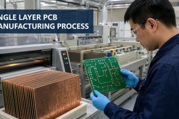
Follow the single layer PCB manufacturing process from DFM and copper imaging through etching, drilling, solder mask, finish and electrical testing.
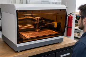
Learn how to make a prototype PCB with a laser engraver using an etch-mask workflow, calibration grid, inspection checks and realistic process limits.
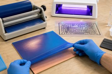
Learn how to apply PCB dry film photoresist, calibrate UV exposure, develop a clean pattern, diagnose defects and prepare files for fabrication.
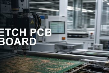
Learn how to etch a PCB board safely, from copper cleaning and resist transfer to etching checks, common failures and when to use factory fabrication.
If you have any enquiry about quotation or cooperation, please feel free to email us at [email protected] or use the following enquiry form. Oursales representative will contact you within 24 hours. Thank you for your interest in our products.