




What PCB Etching Means
To etch a PCB board means to remove unwanted copper from a copper-clad board so only the circuit traces remain. In simple words, you protect the copper you want to keep, expose the copper you want to remove, and use an etchant to dissolve the exposed copper.
This is different from drawing a circuit on paper. The final board must carry current through real copper paths. If a trace is too thin, broken, undercut or accidentally connected to another trace, the board may fail even if the schematic is correct. That is why etching is not only a chemical step. It is also a pattern transfer, cleaning, inspection and safety process.
Hand etching can be useful for learning, quick experiments and very simple one-sided boards. It is not a good match for fine-pitch SMT, controlled impedance, plated through holes, multilayer boards, solder mask, silkscreen or repeatable production. For those cases, a PCB fabrication shop is usually the safer route.
When Home PCB Etching Makes Sense and When It Does Not
Home PCB etching makes sense when the circuit is simple, the trace spacing is generous, the board is one-sided, and the purpose is learning or a rough bench prototype. It does not make sense when the board must be reliable, compact, repeatable or ready for assembly.
| Project type | Home etching fit | Better choice |
|---|---|---|
| Simple LED or sensor circuit | Possible for learning | Home etch or basic prototype PCB |
| Fine-pitch IC board | Poor fit | Factory PCB with solder mask |
| Two-layer board with vias | Difficult to make reliably | Factory fabrication |
| Controlled impedance or RF board | Not suitable | Factory stackup and impedance control |
| Customer sample or production batch | Not recommended | Fabricated PCB or PCBA |
The main decision is not whether etching is possible. It is whether the result will be useful for your next step. If the board is only for learning, a rough etch can teach a lot. If the board must fit components, pass testing or be shared with a supplier, you need manufacturable files and controlled fabrication.
Prepare the Board, Pattern and Safety Setup First
Do not start with chemicals. Start with preparation. You need a clean copper-clad board, a circuit pattern, a resist method, safe handling tools and a place where spills and fumes can be controlled. Etchants vary by region and supplier, so always follow the product label and local disposal rules.
- Copper-clad laminate cut to the required size.
- Printed artwork, toner transfer film, photoresist film or another resist method.
- Gloves, eye protection and good ventilation.
- Plastic tray or container compatible with the etchant.
- Plastic tweezers or holder, not bare hands.
- Clean water for rinsing where allowed by the chemical instructions.
- Labels and a storage plan for used solution and waste.
Never mix chemicals to “make etching faster” unless the process is specifically documented by the chemical supplier and you understand the hazards. Also avoid using kitchen containers or food areas. A PCB etching setup should be treated like a small chemical work process, not a casual craft step.
Clean the Copper So the Resist Can Stick
The resist must stick tightly to the copper. If the copper surface has oil, oxidation, fingerprints or dust, the etchant can creep under the resist and damage the traces. Many failed home-etched boards fail before the board even enters the etchant because the copper was not cleaned properly.
Clean the board with a suitable abrasive pad or cleaner recommended for copper preparation, then remove dust and oils. Handle the board by the edges after cleaning. If you touch the copper with bare fingers, the fingerprint can become a weak spot in the resist.
A simple check is to look at how evenly the surface wets during cleaning. Patchy behavior can mean oil or uneven oxidation is still present. The goal is not to polish the copper for appearance. The goal is a consistent surface that lets the resist hold its edge.
Transfer the Circuit Pattern Without Broken Lines
The transferred pattern is the mask that tells the etchant which copper to keep. If the mask has pinholes, thin areas, shifted artwork or broken traces, the etched PCB will carry those defects into the copper. This is why pattern transfer deserves slow inspection before etching.
For toner transfer, check that all traces are dark, continuous and firmly bonded. For photoresist, check exposure and development so the protected areas remain clean and the unwanted copper is fully open. Do not assume the pattern is correct just because the artwork printed correctly. The board surface may still have gaps or weak edges.
Before etching, compare the board to the layout file. Look especially at IC pads, connector pads, thin traces, ground areas and any point where two traces run close together. Fixing a mask defect before etching is much easier than repairing missing copper later.
Etch the Board Slowly Enough to Control the Result
Etching should remove exposed copper while leaving protected copper intact. The exact time depends on the etchant, temperature, copper thickness, board size, agitation and solution condition. Rushing the process can create undercut traces, uneven copper removal or safety problems.
Place the board into the etching container according to the chemical instructions. Keep the board moving gently if the process requires agitation, and watch the exposed copper areas. Remove the board when the unwanted copper is gone, not when a fixed guessed time has passed.
Do not use metal tools unless the chemical supplier says they are safe with the etchant. Do not heat chemicals casually. Do not leave the process unattended. If the etching is uneven, stop and inspect instead of simply extending the time until the thin traces are attacked.
Rinse, Remove Resist and Inspect the Copper
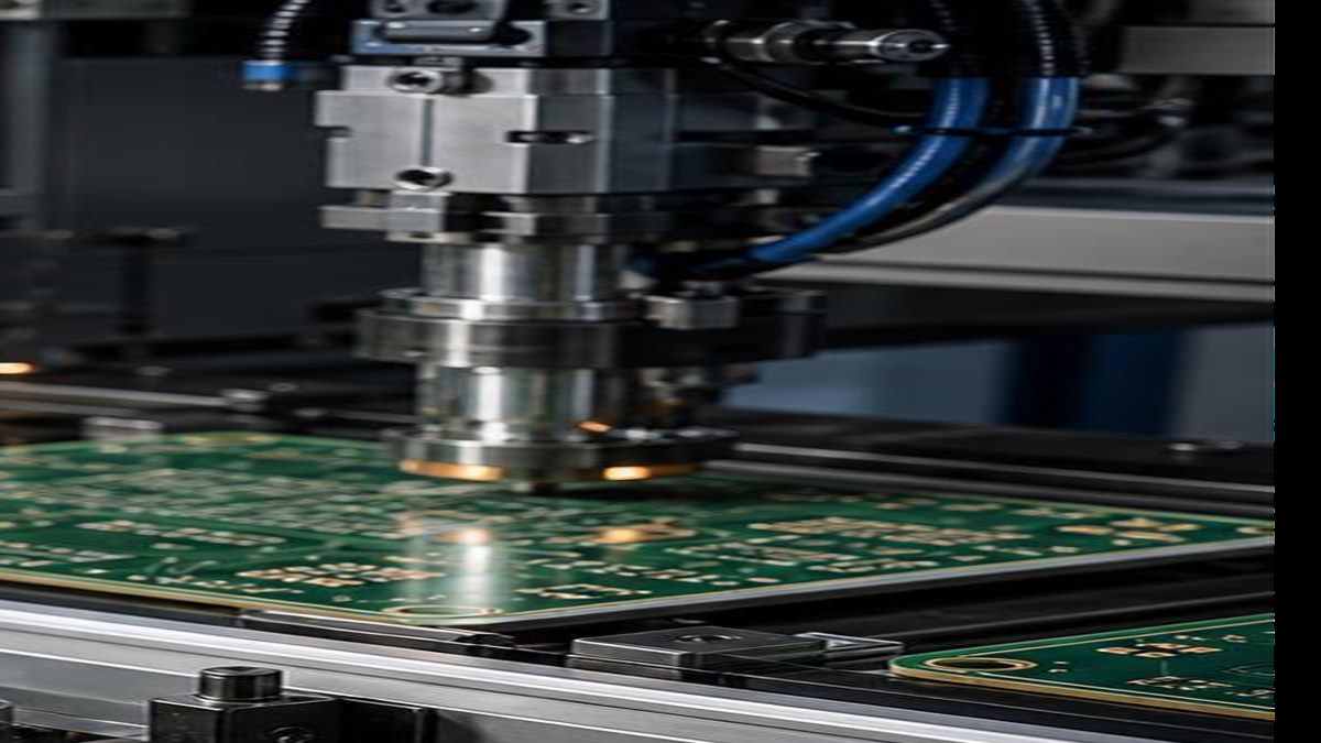
After etching, rinse and neutralize only according to the chemical instructions and local rules. Then remove the resist so the copper traces can be inspected. The board is not finished when the unwanted copper disappears. It is finished only when the remaining copper is continuous, separated and suitable for soldering.
- Check that every trace is continuous from pad to pad.
- Look for copper bridges between close pads or traces.
- Check thin traces for over-etching or broken sections.
- Inspect large copper areas for isolated islands that should not remain.
- Confirm pads are large enough to solder without lifting.
Drill Holes and Check Alignment Before Soldering
If the board uses through-hole parts, drill after etching and before soldering. Hole position matters. A trace may be correct, but if the hole is off-center, the pad can become weak or unusable. For home-etched boards, this is a common point where a visually acceptable board becomes hard to assemble.
Use a suitable small drill and support the board so it does not flex. Drill perpendicular to the board and avoid tearing pads. After drilling, remove dust and inspect every pad. If the pad annular ring is almost gone, soldering may lift the pad or create an unreliable joint.
Factory PCBs solve this with controlled drilling, registration and plated through holes. Home-etched two-sided boards are especially hard because you must align both sides and connect layers without professional plating. If the design needs many vias, it is usually time to use factory fabrication.
Common PCB Etching Failures and How to Read Them
Etching failures usually point back to one of four causes: dirty copper, weak resist, poor artwork transfer or uncontrolled etching. Reading the failure correctly helps you fix the process instead of repeating the same board.
| Failure | What it usually means | What to change next time |
|---|---|---|
| Broken thin traces | Over-etching, weak resist or traces too narrow | Use wider traces and inspect resist edges |
| Copper bridges remain | Under-etching or artwork gap too small | Etch until exposed copper clears; increase spacing |
| Jagged trace edges | Poor transfer or etchant attacking under resist | Clean copper better and improve transfer pressure/exposure |
| Random pinholes | Dust, scratches or weak resist coverage | Clean surface and protect board before etching |
| Pads lift during soldering | Small pads, heat stress or weak laminate | Use larger pads or factory board quality |
Check the Board Electrically Before Installing Parts
Before soldering components, use a multimeter to check the bare etched board. This catches opens and shorts while repair is still easy. Once parts are installed, the circuit becomes harder to diagnose because components create parallel paths.
Check continuity along each important trace. Then check that adjacent traces are not shorted. Pay special attention to power and ground, fine-pitch footprints, connector pads and hand-drilled areas. A board that passes visual inspection can still fail electrically.
If you find a small open trace, it may be possible to repair it with a jumper wire for learning. If you find many opens, bridges or weak pads, do not use that board as proof of the circuit. Fix the etching process or move to a fabricated PCB.
Why Factory PCB Fabrication Is Different from Home Etching
Factory PCB fabrication is not just a cleaner version of home etching. A factory process adds controlled imaging, drilling, plating, solder mask, surface finish, electrical testing and panel control. These steps make the board repeatable and suitable for assembly.
| Need | Home etching limit | Factory advantage |
|---|---|---|
| Two-layer vias | No reliable plated through holes | Drilled and plated vias |
| Fine-pitch SMT | Hard to control trace edge and soldering area | Solder mask and controlled imaging |
| Repeat orders | Manual variation between boards | Repeatable process and inspection |
| Assembly | No paste stencil or assembly data | Gerber, BOM, CPL and inspection flow |
| Reliability | Limited process control | Electrical test and quality checks |
If the goal is a working product, customer sample or production batch, factory fabrication is not a luxury. It is the process that makes the same circuit buildable more than once.
What to Send When You Move from Etching to Fabrication
When your etched board proves the circuit idea, prepare files for a proper PCB fabrication review. A photo of the etched board is useful as context, but it is not enough to manufacture from. The supplier needs design data and build requirements.
- Gerber files for copper, solder mask, silkscreen and board outline.
- NC drill file for holes and slots.
- Board thickness, copper weight and material requirement.
- Surface finish, solder mask color and silkscreen color.
- Minimum trace/space and any critical nets.
- BOM and CPL if the board will be assembled.
- Testing requirement, especially if the etched prototype had a known weak point.
PCBtry can review PCB fabrication files and help turn a hand-etched proof of concept into a manufacturable board. If assembly is also needed, include the BOM, placement file and polarity notes so the PCBA risk can be checked before quotation.
FAQ
Can I etch a PCB board at home?
Yes, but it is best for learning and simple one-sided prototypes. You need proper safety handling, a clean copper surface, a reliable resist pattern and careful inspection. It is not a good substitute for factory fabrication when the board needs fine features, vias, solder mask or repeatable quality.
What chemical is used to etch PCB boards?
Common PCB etchants include ferric chloride and other copper etching solutions, depending on region and supplier. Always follow the product label, safety data and local disposal rules. Do not mix chemicals casually or use undocumented shortcuts to speed up the reaction.
Why are my PCB traces broken after etching?
Broken traces usually come from over-etching, weak resist, dirty copper, traces that are too narrow, or artwork defects. Inspect the transferred pattern before etching and use wider traces for hand processes. If the design needs fine tracks, use factory fabrication.
Can I make a two-sided PCB by etching?
You can attempt it for experiments, but alignment and vias are difficult without factory drilling and plating. Two-sided boards with many vias or tight spacing should usually be fabricated by a PCB manufacturer.
Do I need solder mask on a hand-etched PCB?
A simple etched board can work without solder mask, but solder mask helps prevent solder bridges, protects copper and improves assembly consistency. If the board will be assembled professionally or used repeatedly, a factory PCB with solder mask is usually better.
Should I drill before or after etching?
Most simple hand processes etch first and drill after, so the copper pattern is visible and the pads can guide drilling. The exact method depends on your process, but hole alignment must be checked before soldering.
Can I use an etched PCB for production?
It is not recommended. A hand-etched PCB has limited process control, no plated through holes, no normal solder mask process and poor repeatability. Use it to prove a circuit, then move to factory fabrication for production.
What files does a PCB factory need after my etched prototype works?
Prepare Gerber files, NC drill files, board specifications and any critical notes. For assembly, also send the BOM, CPL, polarity notes and testing requirements. These files let the supplier check manufacturability instead of guessing from photos.
Final Advice Before You Etch or Order
Etching a PCB board is a useful way to learn how copper patterns become real circuits, but the process has limits. Clean the copper, transfer the pattern carefully, etch under control, inspect the traces and test the bare board before installing parts. If the design needs fine spacing, vias, solder mask, assembly or repeatability, prepare proper fabrication files instead of trying to force a home process beyond its safe range.
When you are ready to move from a hand-etched prototype to a manufacturable PCB, send PCBtry the Gerber files, drill file, board specifications and assembly files if needed through the contact page. A clear file package makes it easier to check DFM risk, quote the board and avoid repeating the same prototype mistakes in production.



0 Comments