Blog
How Does a PCB Board Work? Copper Paths, Layers and Component Roles
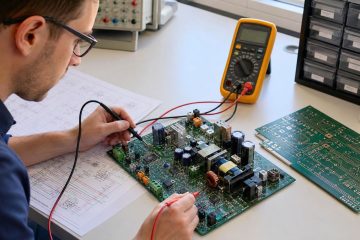
Learn how a PCB supports components and routes power, ground and signals through copper traces, pads, vias and layers, with a simple circuit walkthrough.



Learn how a PCB supports components and routes power, ground and signals through copper traces, pads, vias and layers, with a simple circuit walkthrough.
Learn how PCB etch factor changes finished trace width, impedance and fine-line DFM, with formulas, examples and fabrication checks.
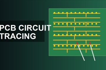
Learn how to trace a PCB circuit by following visible tracks, using continuity mode correctly, marking nets, checking components and preparing repair or remake notes.
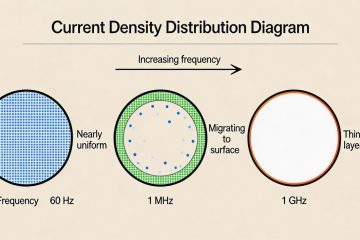
Introduction: The Hidden Challenge in High-Frequency Circuit Design In the world of electronics, once a signal’s frequency crosses a certain threshold, physical phenomena that are virtually invisible at DC or low frequencies begin to surface — profoundly influencing circuit performance and reliability. Skin effect is one of the most critical among them. Read more
If you have any enquiry about quotation or cooperation, please feel free to email us at [email protected] or use the following enquiry form. Oursales representative will contact you within 24 hours. Thank you for your interest in our products.