




Introduction: The Hidden Challenge in High-Frequency Circuit Design
In the world of electronics, once a signal’s frequency crosses a certain threshold, physical phenomena that are virtually invisible at DC or low frequencies begin to surface — profoundly influencing circuit performance and reliability. Skin effect is one of the most critical among them. Whether you are designing a high-speed router motherboard or optimizing the efficiency of a switch-mode power supply, ignoring the skin effect can lead to catastrophic consequences — signal attenuation, impedance mismatch, and unexpected hotspots.
This article serves as your definitive guide. We will not only thoroughly explain the origins and principles of skin effect in PCB traces, but also provide a set of practical PCB design strategies you can apply immediately.
Core Principles — When Alternating Current Meets Electromagnetic Fields
What Is Skin Effect?
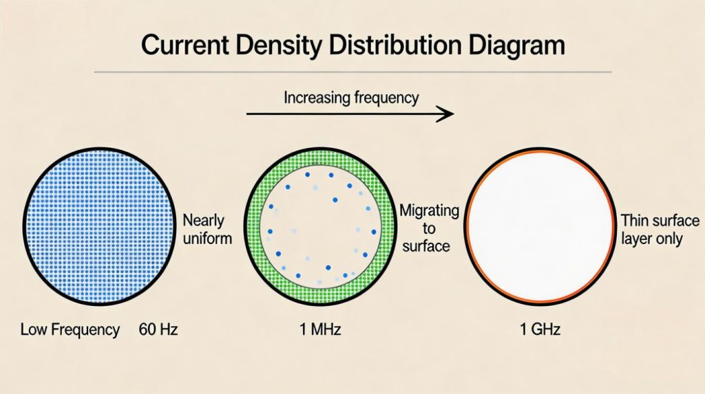
Simply put, skin effect refers to the phenomenon where an alternating current (AC) flowing through a conductor no longer distributes uniformly across its entire cross-section. Instead, the current density tends to concentrate near the surface — the “skin” — of the conductor. The higher the frequency, the more pronounced this concentration becomes.
Physical Origin: A Four-Step Explanation
This phenomenon is a direct consequence of Faraday’s Law of Electromagnetic Induction:
- Alternating current flowing through a conductor generates a constantly changing magnetic field both inside and around it.
- According to Faraday’s Law, this changing magnetic field induces eddy currents within the interior of the conductor.
- The eddy currents are oriented such that they oppose the original current at the center of the conductor, but reinforce it at the surface.
- The net result is that current at the center is partially canceled out, while current at the surface is enhanced — producing the characteristic “crowding” effect toward the surface.
The diagram below clearly illustrates the current density distribution across a conductor’s cross-section at different frequencies:
Key Parameter: Skin Depth (δ)
We use skin depth (δ) to quantify the skin effect. It is defined as the depth at which the current density drops to 1/e (approximately 37%) of its surface value. The formula for skin depth is:
Where:
- ρ (rho) — Resistivity of the conductor (for copper, ρ ≈ 1.68 × 10⁻⁸ Ω·m)
- μ (mu) — Magnetic permeability of the conductor (for non-magnetic materials like copper, μ ≈ 4π × 10⁻⁷ H/m)
- f — Frequency of the current (Hz)
- ω = 2πf — Angular frequency
Two critical conclusions emerge immediately from this formula:
- Frequency is the dominant factor. Skin depth δ is inversely proportional to the square root of frequency. Higher frequencies yield smaller skin depths.
- Material properties set the intrinsic limit. For a given material (fixed ρ and μ), the only levers you have are frequency and geometry.
For a copper conductor:
| Frequency | Skin Depth (δ) |
|---|---|
| 50 Hz (power line) | ~9.3 mm |
| 1 MHz | ~66 µm |
| 1 GHz | ~2.1 µm |
| 28 GHz (5G mmWave) | ~0.38 µm |
At high frequencies, current effectively flows through only an infinitesimally thin surface layer.
Real-World Impacts on PCB Design — Four Critical Consequences
Understanding the physics leads us to the more practical question: What does this actually mean on a PCB?
1. Increased Effective Resistance and Conductor Loss
Because the effective cross-sectional area available for current flow is drastically reduced, the effective AC resistance of the conductor rises significantly above its DC resistance. This directly causes:
- DC voltage drop and power dissipation: For high-current power traces, increased resistance leads to greater voltage drops and I²R heating, reducing power supply efficiency and potentially creating localized hotspots.
- High-frequency signal attenuation: For high-speed digital or RF signals, conductor loss is one of the primary sources of signal degradation, directly limiting maximum transmission distance and quality.
2. Changes in Characteristic Impedance
The characteristic impedance of a PCB trace depends on its per-unit-length inductance, resistance, capacitance, and conductance. The skin effect-induced changes in resistance and internal inductance cause the actual trace impedance to deviate from values calculated using DC resistance and external inductance. In high-speed designs, such deviations lead to impedance mismatch, which in turn causes signal reflections.
3. Signal Integrity Degradation
For high-speed digital signals (e.g., DDR memory buses, PCIe, USB 3.0), the signal contains rich high-frequency components. The frequency-dependent loss caused by the skin effect severely “smears” signal edges, manifesting as:
- Eye diagram closure: At the receiver, the “eye” opening shrinks, reducing the decision margin.
- Rise/fall time degradation: Transitions from logic ‘0’ to ‘1’ become sluggish.
This directly lowers the maximum achievable operating frequency and timing margin of the system.
4. Non-Uniform Current Distribution and Localized Heating
Skin effect inherently creates non-uniform current density on the surface. When combined with right-angle corners or abrupt width changes in PCB traces, current crowding intensifies at these locations, generating hot spots. Over time, this can compromise board reliability.
Design in Practice — 7 Techniques to Combat Skin Effect
As PCB designers, we are far from powerless. The following techniques help you proactively manage the impact of skin effect.
1. Optimize Trace Geometry
This is the most direct and effective approach.
- Increase trace width: For traces that must carry high-frequency or high current, widening the trace (where space permits) increases the total surface area, thereby reducing per-unit-length AC resistance.
- Consider flat copper ribbons: In extreme high-frequency or high-power applications, consider using a flatter rectangular cross-section (as seen in certain microstrip lines or power modules) to maximize surface area.
2. Select Conductor Materials Carefully
Theoretically, using a material with lower resistivity (e.g., silver plating) can reduce losses. However, in practical PCB fabrication:
- Cost is the primary concern: Whole-board silver plating is not economically viable.
- Oxidation issues: Silver oxidizes and darkens in air, potentially affecting contact resistance.
- Practical solution: For extremely critical high-frequency traces, selective gold plating (e.g., the gold layer in ENIG surface finish) can be applied after etching to protect the surface and reduce high-frequency losses, though this comes at a premium.
3. Control Dielectric Thickness and Layer Stackup
While the dielectric does not directly affect skin depth, it influences per-unit-length capacitance and inductance, which together determine characteristic impedance. A stable, low-loss dielectric layer (e.g., Rogers materials) paired with a well-designed stackup helps you more accurately predict and compensate for impedance changes caused by the skin effect.
4. Use Parallel Traces or Reference Planes
Providing high-speed signals with a tightly coupled, continuous reference plane (ground or power plane) is essential. This not only effectively controls impedance but also provides a low-impedance return path for high-frequency return currents, reducing additional losses and radiation caused by high-impedance return paths.
5. For Power Designs: Focus on “Effective” Current-Carrying Capacity
When calculating current-carrying capacity for high-current traces, you can no longer simply use DC current ratings. Refer to modern standards such as IPC-2152, which account for the skin effect and proximity effect at high frequencies (e.g., ripple currents in switch-mode power supplies) and apply appropriate derating factors. This is critical for power PCB design.
6. Leverage Simulation Tools for Prediction
For GHz-level high-speed designs or precision power designs, electromagnetic simulation tools (such as ANSYS SIwave, Cadence Sigrity, or Altium Designer’s SI/PI Analyzer) are strongly recommended.
- Advantage: These tools calculate the actual AC resistance, loss, and impedance while accounting for skin effect and conductor roughness, allowing you to predict performance and optimize designs before fabrication.
7. Manufacturing Considerations: Copper Foil Roughness
This is a frequently overlooked but absolutely critical factor. Real-world copper foil surfaces are not perfectly smooth; they have microscopic roughness (Rz). At high frequencies, current travels along the undulating, rough surface, effectively lengthening the current path and further increasing conductor losses. In some cases, the impact of roughness can exceed that of the skin effect itself.
- Design countermeasure: For high-speed designs, specify low-profile or ultra-low-profile copper foil (e.g., HVLP or VLP) and include this requirement in your fabrication notes.
Frequently Asked Questions (FAQ)
Does the skin effect only exist in high-frequency circuits? Above what MHz should I start worrying about it?
Strictly speaking, any AC current exhibits skin effect. However, in engineering practice, a “significant frequency” threshold exists. A common rule of thumb is that when the trace width exceeds five times the skin depth, the current distribution can still be approximated as uniform. For standard 1-oz (35 µm) copper, the skin effect begins to warrant serious attention at approximately 10 MHz and above.
Does DC current have skin effect?
No. DC current distributes uniformly across the entire conductor cross-section because its magnetic field is constant, and therefore cannot induce eddy currents within the conductor.
Do inner-layer traces in multilayer boards also suffer from the skin effect?
Absolutely. Skin effect is independent of whether a trace is on the top, bottom, or an inner layer — it depends solely on the frequency of the current it carries. Inner-layer traces, being sandwiched between dielectric layers, often have poorer thermal dissipation, making the increased resistance and heating caused by the skin effect even more critical to monitor.
How can I quickly estimate whether my design needs to consider skin effect?
Perform a quick calculation: use the formula to determine the skin depth δ corresponding to the highest frequency component of your signal. Then compare this δ to your trace’s copper thickness (e.g., 35 µm for 1 oz). If δ is close to or smaller than the trace thickness, you absolutely need to account for it.
Besides traces, are vias on a PCB also affected by the skin effect?
Yes. The metalized barrel of a via carries high-frequency current and is subject to the same skin effect, manifesting as increased barrel resistance. In extremely high-frequency designs, this can even affect the via’s insertion loss and return loss.
Conclusion: Turning Skin Effect from a Challenge into a Design Advantage
The skin effect is a fundamental law of the high-frequency domain. We cannot eliminate it, but we can master it through deep understanding. We have reviewed its essence — electromagnetic fields forcing current to the surface — and its impacts — rising resistance, shifting impedance, increasing losses. We have also explored a suite of countermeasures — optimizing geometry, managing materials, controlling roughness, and leveraging simulation.
As a modern electronics engineer or designer, internalizing skin effect knowledge means you can anticipate problems early, mitigate risks, and make more robust, efficient design decisions. Starting with your next high-speed or power project, examine your critical traces, apply the techniques in this article, and you will navigate the currents of high-frequency design with greater confidence.
Take action now: Open your current design, locate a clock signal or power switching node, calculate the skin depth using the formulas above, and determine whether it has become a factor you need to address.



0 Comments