




To choose electronic components for PCB design, start with the circuit function, then check electrical ratings, package size, footprint accuracy, availability, lifecycle, assembly process limits, thermal performance, and BOM documentation. A part that looks correct in the schematic can still create PCB layout, soldering, sourcing, testing, or quote problems if these checks are skipped.
The best component choice is not always the smallest, cheapest, or highest-rated part. For a manufacturable PCB, each component must fit the electrical requirement, the board space, the assembly process, the supply chain, and the testing plan. This guide shows a practical selection workflow for engineers, product teams, and buyers preparing a custom PCB or PCBA quote.
What should you decide before choosing PCB components?
Before selecting individual parts, define what the board must do. Component selection becomes much easier when the voltage, current, signal speed, operating environment, enclosure limits, expected quantity, assembly method, and test requirements are already known.
- Input voltage and tolerance range
- Maximum current and load behavior
- Signal frequency, bandwidth, or data rate
- Required interfaces and connector positions
- Board size, height limits, and mounting method
- Operating temperature and vibration exposure
- Prototype quantity and future production volume
- Manual assembly, SMT assembly, or mixed assembly needs
- Inspection, programming, and functional test requirements
If the project will be sent for manufacturing, keep the design specification and BOM aligned from the start. A custom board quote usually depends on both PCB fabrication data and component decisions. For file preparation, this guide to making a custom PCB is a useful companion.
How do electrical ratings guide component selection?
Electrical ratings are the first filter. A component should be selected with enough margin for voltage, current, power, temperature, tolerance, signal speed, and environmental stress. Do not choose parts only by nominal values shown in a reference circuit.
| Component Type | Main Ratings to Check | Common Mistake |
|---|---|---|
| Resistor | Resistance, tolerance, power, voltage, temperature coefficient | Using a package that cannot dissipate enough power |
| Capacitor | Capacitance, voltage, dielectric, ESR, ripple current, DC bias | Ignoring capacitance loss under DC bias |
| Diode | Reverse voltage, forward current, surge current, recovery speed | Selecting a slow diode in a switching circuit |
| MOSFET | VDS, current, RDS(on), gate charge, thermal resistance | Reading current rating without checking PCB heat path |
| IC | Supply range, IO voltage, package, thermal pad, timing, layout notes | Skipping datasheet layout recommendations |
| Connector | Current rating, pitch, mating cycle, orientation, mechanical load | Choosing a connector that fits electrically but fails mechanically |
Use the latest datasheet, not only an online symbol or copied reference design. Check absolute maximum ratings, recommended operating conditions, application circuits, layout notes, and package drawings. For new designs, build margin into the part choice so normal tolerance, temperature, and load variation do not push the component to its limit.
Why do footprints and package sizes matter?
Footprint mistakes are one of the most common reasons a PCB prototype fails. The schematic symbol may be correct, but the board can still be wrong if the pad number, pin-one orientation, body size, courtyard, exposed pad, or connector direction is incorrect.
Before locking the design, verify these footprint details:
- Pad number mapping against the datasheet package drawing
- Pin-one orientation on symbol, footprint, silkscreen, and assembly drawing
- Pad size and solder mask opening for the selected assembly process
- Component height and clearance inside the enclosure
- Connector mating direction and cable access
- Thermal pad size, stencil opening, and via strategy
- Courtyard clearance for pick-and-place and inspection access
Small packages can save board space, but they may increase assembly cost and inspection difficulty. For early prototypes, choosing a slightly larger package can make rework and debugging easier. For production, package choice should match the SMT process and inspection method. See DFM and DFA in PCB manufacturing for manufacturability checks.
How should availability and lifecycle affect the BOM?
A technically suitable component is not a good production choice if it is unavailable, obsolete, single-sourced, or difficult to substitute. Check availability before the PCB layout is finalized, not after the Gerbers are ready.
| BOM Risk | What to Check | Buyer Action |
|---|---|---|
| Low stock | Current distributor inventory and factory lead time | Add an approved alternate or redesign early |
| End-of-life risk | Lifecycle status, PCN notices, recommended replacement | Avoid for new designs unless unavoidable |
| Single source | Whether another supplier or package can replace it | Document risk and keep buffer stock |
| Unclear substitute | Electrical, package, tolerance and certification differences | Approve substitutions in writing before assembly |
| Counterfeit risk | Supplier channel and traceability | Use controlled sourcing for critical ICs |
For PCB assembly, the BOM should include manufacturer part number, quantity, package, value, tolerance, voltage rating, approved substitutes, do-not-fit notes, and sourcing responsibility. If the manufacturer is expected to source parts, make that clear in the RFQ. For assembly scope, review turnkey PCB assembly.
Which components need thermal or signal checks?
Power parts, high-speed parts, RF parts, clocks, connectors, and protection devices need more than a basic value check. They affect layout, copper area, return paths, testing, and sometimes the PCB stackup.
- Power regulators: check heat dissipation, switching loop size, inductor rating, diode/MOSFET losses, and input/output capacitor selection.
- High-current connectors: check contact rating, trace width, copper weight, temperature rise, and mechanical strain relief.
- Crystals and oscillators: check load capacitance, placement, ground reference, and routing length.
- Differential interfaces: check impedance, pair spacing, reference plane continuity, length matching, and connector pinout.
- ESD and surge protection: place protection near connectors and verify capacitance, clamping voltage, and current rating.
- RF parts: verify footprint geometry, land pattern, grounding, material choice, and controlled impedance needs.
Component choice and PCB layout are connected. If a component requires a special footprint, thermal pad, keep-out area, controlled impedance, or test access, it should be planned before routing begins. Otherwise the PCB may need a late redesign.
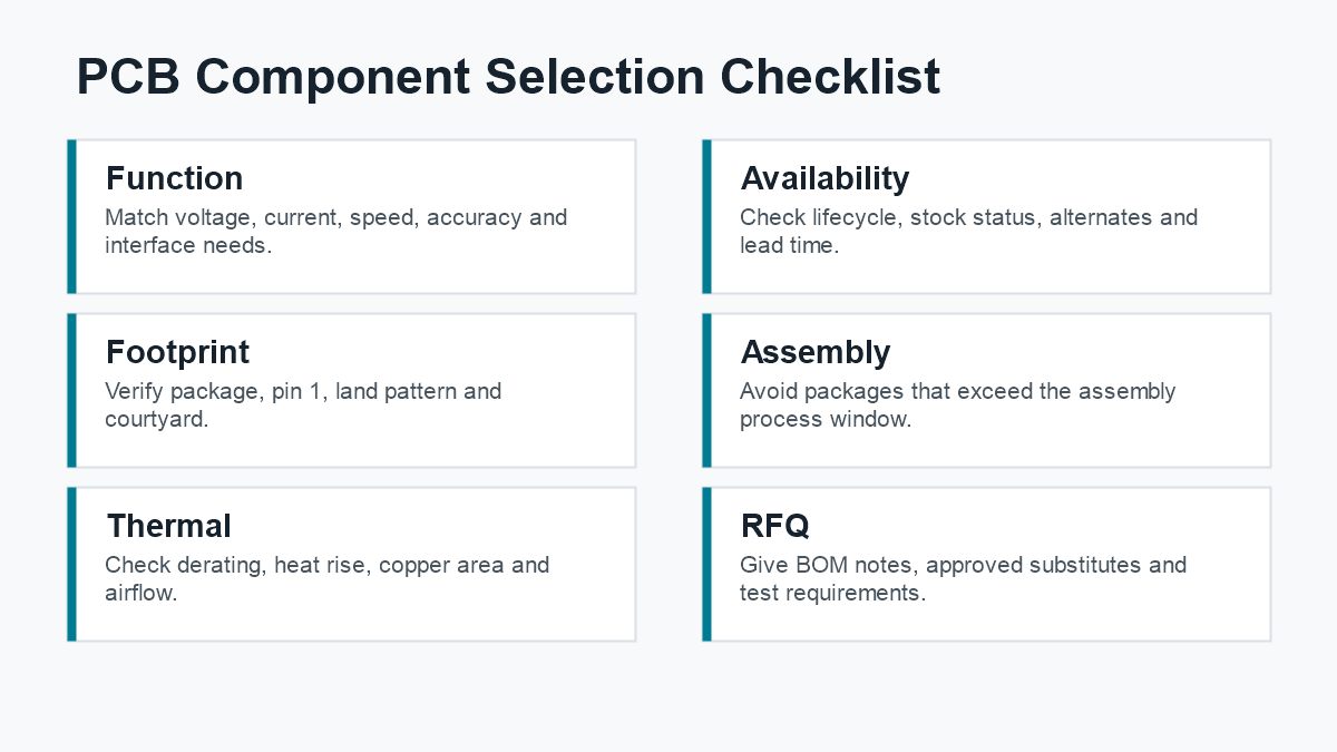
PCB component selection checklist
| Check | Pass Condition |
|---|---|
| Function | The part meets the required circuit function and interface needs. |
| Electrical margin | Voltage, current, power and temperature ratings have realistic margin. |
| Package | The package can be assembled, inspected and reworked for the project stage. |
| Footprint | Pin numbers, pad geometry, pin-one mark and courtyard match the datasheet. |
| Availability | The part is in stock or has approved alternates for production. |
| Lifecycle | The part is not obsolete or risky for a new design. |
| Thermal | Power loss, copper area, airflow and derating are checked. |
| Testing | Important rails, signals and programming points are accessible. |
| BOM | MPN, value, package, quantity and approved substitutes are clear. |
What BOM notes help manufacturers quote the PCB correctly?
Manufacturers quote more accurately when the BOM states not only what parts are used, but also which choices are fixed, which alternatives are allowed, and what assembly or testing risks must be considered.
- Exact manufacturer part numbers for critical parts
- Approved substitutes for passive components and standard ICs
- Do-not-fit and optional component notes
- Polarity and orientation notes for LEDs, diodes, electrolytic capacitors and connectors
- Special handling for moisture-sensitive, ESD-sensitive or expensive parts
- Programming, calibration, conformal coating or functional test requirements
- Whether components are turnkey sourced, consigned, or mixed
Send the BOM together with Gerber or ODB++ files, drill files, assembly drawing and CPL/centroid data. If the board is already ready for production, this Gerber file preparation guide can help check the manufacturing package.
How can PCBTRY support component-ready PCB projects?
PCBTRY can review PCB manufacturing files and assembly-related documentation before prototype or production orders. The practical value is not only making the board; it is identifying component, footprint, DFM, BOM, and assembly risks before they become failed prototypes or quote revisions.
For a component-ready PCB quote, send Gerber files, drill files, BOM, CPL, assembly drawing, quantity, material, surface finish, copper weight, delivery target, and testing requirements to [email protected]. PCBTRY can review the package and provide manufacturing or assembly feedback before you approve production.
FAQs about choosing electronic components for PCB design
What is the first step in choosing PCB components?
The first step is defining the circuit requirements: voltage, current, signal speed, interface type, operating temperature, board size, assembly method and expected quantity. Without these limits, component choices may look correct but fail during layout, sourcing or production.
Should I choose components before or after PCB layout?
Choose the main components before PCB layout, then refine details during placement and routing. The package, footprint, connector direction, thermal pad and keep-out area affect the board outline, routing space and manufacturing rules.
How much voltage margin should a component have?
There is no single margin for every circuit, but components should operate within recommended conditions, not near absolute maximum ratings. Power, temperature, surge and transient conditions should be considered, especially for capacitors, MOSFETs, diodes and connectors.
Why is footprint verification important?
A wrong footprint can make a PCB impossible to assemble even when the schematic is correct. Always compare pad numbers, package dimensions, pin-one orientation, exposed pad and recommended land pattern with the latest datasheet.
What does an approved substitute mean in a BOM?
An approved substitute is a replacement part that the engineer or buyer has already accepted. It should match the required value, package, tolerance, voltage, current, temperature and function. Substitutes should be approved before assembly begins.
Are smaller components always better for PCB design?
No. Smaller packages save space but may increase assembly cost, inspection difficulty and rework risk. For prototypes, slightly larger packages can make debugging and manual repair easier. Use small packages only when the design or production need justifies them.
Which PCB components need thermal checking?
Voltage regulators, MOSFETs, power resistors, LEDs, high-current connectors, motor drivers and power ICs need thermal checks. Review power loss, copper area, airflow, ambient temperature and package thermal resistance.
How do component choices affect PCB cost?
Component choices affect PCB cost through package size, assembly difficulty, sourcing risk, inspection needs, rework probability and required board features. Fine-pitch ICs, BGAs, heavy-current parts and special connectors can raise cost beyond the component price.
What should I send to a PCB manufacturer for review?
Send Gerber or ODB++ files, drill files, BOM, CPL, assembly drawing, stackup notes, quantity, material, finish, copper weight and testing requirements. The manufacturer can then check fabrication, assembly and sourcing risks together.
Can a PCB manufacturer help select components?
A PCB manufacturer can usually help identify manufacturability, footprint, sourcing and assembly risks, but the circuit designer remains responsible for electrical function. For critical choices, combine datasheet review, engineering validation and manufacturer DFM feedback.


