





The metal core PCB manufacturing process bonds a copper circuit to a metal heat-spreading base through an electrically insulating, thermally conductive dielectric. The construction is common in LED lighting, power conversion, motor control and other assemblies that must move heat toward a chassis or heatsink. Unlike an ordinary FR-4 board, the metal base is conductive and mechanically different, so dielectric integrity, metal preparation, isolation features, flatness and profiling need dedicated controls.
Thindry can review the stackup, Gerber data, drill files, drawing and thermal/electrical requirements before fabrication. Send those files with quantities, copper and base-metal requirements, surface finish, isolation voltage requirement and assembly interface details for an engineering review and quotation. Final material and test limits must be agreed for the actual product; a generic “high thermal conductivity” label is not an acceptance specification.
What Is a Metal Core PCB Manufacturing Process?
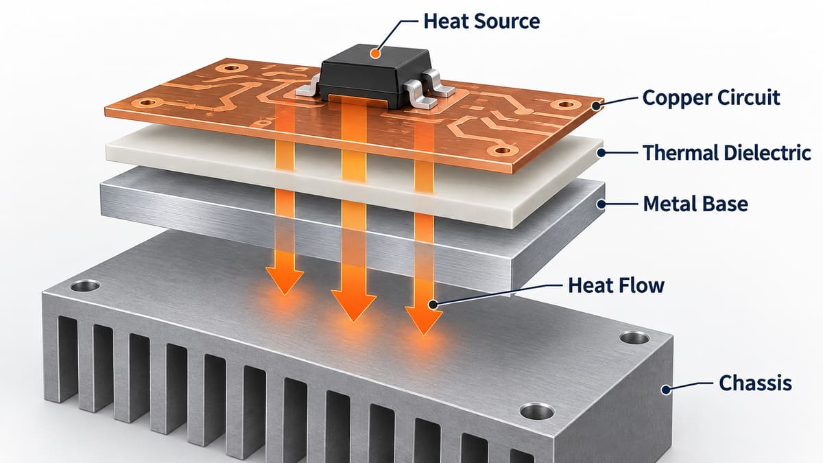
A metal core PCB, also called an insulated metal substrate or MCPCB, normally combines a patterned copper circuit, a thin dielectric and an aluminum or copper base. Heat passes from the component pad through the copper and dielectric into the metal spreader, while the dielectric prevents the circuit from shorting to that metal.
The process is difficult because the same dielectric must provide two competing outcomes: low resistance to heat flow and adequate electrical isolation. Its thickness, filler system, cure, bond quality and local damage matter more than the base-metal conductivity alone. The finished board must also fit and contact the mechanical heat path; a thermally capable laminate can still perform poorly if it is bowed or mounted across an air gap.
How Does the Metal Core PCB Manufacturing Process Work?
The factory sequence converts an approved construction into a patterned, insulated and mechanically finished board. Each stage needs a defined input, process control, defect reaction and release record.
1. Engineering Review and Stackup Release
Fabrication begins by reconciling Gerber or ODB++ data, drill files, outline, drawing, copper weight, dielectric identity, base-metal type and all electrical or thermal acceptance requirements. The engineer also confirms whether holes are non-plated, electrically isolated, connected to copper, or part of a special multilayer construction. Ambiguous holes and an unspecified dielectric can produce a board that matches the artwork but not the safety or thermal design. A released stackup and documented DFM answers are the buyer evidence.
2. Metal Base and Dielectric Material Preparation
The metal panel is checked for identity, thickness, surface condition and flatness, then cleaned or treated for bonding. Oil, oxide, scratches or embedded debris can interrupt adhesion or create a thin spot. The dielectric and copper foil must match the approved material system and storage requirements. Incoming lot identity and the supplier’s controlled datasheet matter more than a conductivity number copied into an email.
3. Dielectric Bonding and Copper Lamination
The dielectric and copper are bonded to the prepared metal under a material-specific temperature, pressure and time cycle. The goal is continuous adhesion and insulation without voids, contamination or excessive flow. Poor bonding can increase local thermal resistance, cause delamination during soldering or weaken voltage isolation. The press recipe, material lot and any specified bond or dielectric checks provide traceable evidence.
4. Circuit Imaging and Copper Etching
Photoresist defines the circuit, and exposed copper is etched away while the dielectric and metal-backed panel are protected. Copper thickness, trace geometry and large copper-density differences affect etch compensation. Over-etching narrows tracks; under-etching leaves shorts or insufficient spacing. Artwork inspection and finished-copper verification should be tied to the drawing, not to a generic shop rule.
5. Drilling, Isolation and Special Hole Processing
Mechanical holes, mounting features and any plated structures are produced using a route appropriate to the construction. A drill that reaches conductive metal can create burrs, dielectric damage or an unintended circuit-to-core path. Some designs require oversized openings, dielectric isolation and a separate plated-hole build; that is not equivalent to drilling a standard FR-4 through-hole. Cross-section or insulation evidence may be appropriate when the hole construction is critical.
6. Solder Mask, Legend and Surface Finish
Solder mask protects the circuit and controls solderable openings, while the selected finish protects exposed copper pads. Registration matters around LED thermal pads, fine clearances and mounting holes. Mask in a heat-transfer or chassis-contact area can change the interface; finish choice affects solderability and assembly process compatibility. Buyers should release exact mask openings and finish requirements rather than relying on a product-family default.
7. Profiling, V-Scoring and Edge Control
Metal-backed panels require suitable routing or scoring tools and controlled support. Tool wear, score depth, burrs and local deformation can change outline fit, flatness or electrical clearance to the core. Sharp metal edges also create handling and assembly risk. Dimensional inspection should include the mounting and heat-sink interface features that control final contact.
8. Electrical, Insulation and Visual Inspection
Bare-board electrical test checks the intended copper network; an agreed insulation or withstand test checks a different risk between circuit and metal. Visual and automated inspection examine pattern, mask, finish and damage, but they do not prove a thermal path. Test voltage, dwell, leakage limit and sampling must come from the product requirement and material/construction capability—not from a universal internet value.
9. Thermal and Mechanical Verification
Where thermal performance is contractual, the method must define the specimen, heat path, interface material, clamping, sensor position and calculation. A laminate datasheet value is not the same as finished-board or junction-to-ambient thermal resistance. Flatness and mounting contact should also be verified where they control assembly performance. The release report should state exactly what was measured.
What Materials Are Used in Metal Core PCB Manufacturing?
Material selection starts with the complete heat and insulation path, not with the metal name. Aluminum is widely used for weight, machinability and commercial balance; copper can spread heat more effectively but changes mass, cost and processing. The dielectric must be selected by its qualified thickness, thermal resistance or conductivity, voltage behavior, adhesion and temperature exposure.
| Construction decision | Engineering effect | What to place on the RFQ/drawing |
| Aluminum or copper base | Heat spreading, stiffness, mass, machining and cost | Material/grade if controlled, finished thickness and exposed-edge requirements |
| Dielectric system | Through-thickness thermal resistance and electrical isolation | Named material or approved equivalent, thickness and required test limits |
| Copper thickness | Current capacity, heat spreading, etch geometry and soldering | Finished copper and critical feature dimensions |
| Surface finish | Solderability, shelf handling and assembly compatibility | Finish type and any restricted contact/thermal areas |
| Interface to heatsink | Contact resistance can dominate the system result | Flatness/contact requirements, mounting pattern and interface material assumptions |
For a broader sourcing comparison, see the aluminum PCB material and quote checks. Do not substitute one dielectric based only on the same nominal W/m·K value; thickness, test method and electrical/mechanical properties can differ.
How Is the MCPCB Stackup Designed?
The simplest stackup is copper, dielectric and metal base. More complex constructions can add copper layers or local isolation structures, but every added dielectric and interface changes heat flow and manufacturability. The stackup drawing should define layer order, finished thicknesses, copper, dielectric, metal, finish and controlled tolerances.
Start from component loss and allowable temperature, map the intended path to the chassis, then allocate thermal resistance across the solder joint, copper spreading, dielectric, metal base and interface. This prevents the common mistake of treating the metal plate as the whole solution. If the design uses thermal vias before heat reaches the metal-backed region, review the thermal-via design checks as a separate part of the path.
What Are the Key Manufacturing Challenges?
The most consequential challenges are hidden at interfaces or created during metal handling. They may escape a cosmetic inspection and appear only during soldering, voltage stress or powered thermal testing.
| Risk | Process source | Possible result | Useful control/evidence |
| Dielectric void or thin spot | Contamination, surface damage or bonding variation | Hotspot, weak isolation or delamination | Material/press traceability and agreed insulation or section checks |
| Circuit-to-core short | Burr, misregistration or incorrect hole isolation | Immediate or stress-dependent electrical failure | Hole construction review and circuit-to-core test |
| Trace geometry loss | Etch variation, especially with heavier copper | Clearance or current-path nonconformance | Finished-feature inspection against released artwork |
| Bow or damaged interface | Lamination stress, handling or profiling | Poor heatsink contact and uneven assembly | Flatness and mounting-surface inspection |
| Edge burr | Worn tooling or unsupported routing/scoring | Fit, handling or insulation-clearance risk | Tool control and edge/outline inspection |
How Does Design Affect Manufacturing Reliability?
Design determines whether the dielectric can remain intact and whether the finished board can be tested and mounted repeatably. Keep copper and pads clear of conductive edges according to the agreed fabrication capability, define isolation around holes, avoid unspecified mask in thermal contact areas and provide tooling or fiducials suited to the assembly process.
A practical design review also checks copper balance, heavy-component support, LED or power-device pad geometry, connector forces and chassis tolerances. The board drawing should identify electrically critical clearances and thermally critical surfaces. If these are left implicit, the factory cannot know which ordinary variation becomes a product failure.
What Tests Ensure MCPCB Quality and Reliability?
No single test proves both electrical insulation and thermal performance. Build the test plan from the failure modes and distinguish material qualification, process monitoring, bare-board acceptance and assembled-system validation.
| Check | What it can show | What it cannot prove alone |
| Network electrical test | Specified opens and shorts in the copper circuit | Thermal resistance or all circuit-to-core insulation behavior |
| Circuit-to-core insulation/withstand | Performance under an agreed electrical stress | Long-term life outside the defined conditions |
| Dimensional and flatness inspection | Fit, mounting and interface geometry | Powered component temperature |
| Cross-section or bond evaluation | Selected internal construction and interface evidence | Every location on every production board |
| Thermal measurement | Result for a defined sample, fixture and boundary condition | A different assembly, heatsink, airflow or interface |
| Thermal cycling or application stress | Construction response to the specified stress sequence | Unspecified field conditions or unlimited lifetime |
Acceptance criteria should identify method, limit, sample plan and reaction to failure. “Thermally tested” without those four items is not decision-grade evidence.
How Long Does Metal Core PCB Manufacturing Take?
Lead time depends on material availability, construction maturity, panel and tooling needs, copper thickness, special hole isolation, finish, profiling and the required test plan. A first build may need added time for stackup confirmation, material procurement, tooling and report review; repeat orders can move faster only when the same controlled inputs remain valid.
For a useful schedule, separate engineering release, material readiness, fabrication, test and buyer approval. Ask the supplier to identify the current critical path rather than promising a universal prototype or mass-production number.
How Do You Choose a Reliable Metal Core PCB Manufacturer?
Choose the manufacturer by how clearly it controls the construction and proves the result. A capable supplier should be able to explain which parameters come from the material system, which are measured on the finished board, and which belong to the assembled thermal system.
- Can engineering issue a controlled stackup and resolve metal-contact and hole-isolation questions?
- Can the supplier identify the dielectric and base material by lot and approved specification?
- Are bonding, etching, metal machining and burr controls specific to MCPCB work?
- Can it state the coverage and limits of electrical, insulation, dimensional and thermal tests?
- Will first-article reports identify the exact revision, construction and acceptance criteria?
- Can fabrication feedback connect to assembly, heatsink mounting and powered validation?
Use the metal core PCB manufacturing service page to compare available fabrication support with your project requirements, then verify every critical requirement in the quotation and drawing.
What Should Be Included in an MCPCB RFQ?
A quote is technically comparable only when every supplier receives the same construction and acceptance package.
- Gerber or ODB++, NC drill/rout files and readme.
- Fabrication drawing with dimensions, tolerances, scoring and edge requirements.
- Stackup with copper, dielectric, metal type and finished thickness.
- Named dielectric or approved-equivalent rules and controlled thermal/electrical properties.
- Hole table identifying plated, non-plated, metal-connected and isolated structures.
- Solder mask, legend and surface-finish requirements.
- Electrical network, circuit-to-core insulation and any thermal test requirements.
- Quantity, panel/array preference, assembly process and mounting/heatsink assumptions.
- Required first-article, material, inspection and test reports.
Frequently Asked Questions
Is a metal core PCB always made with aluminum?
No. Aluminum is common, but copper and other metal-base options exist. Select the base with the full thermal, mechanical, mass, machining and cost requirements—not one conductivity number.
Is the metal core electrically connected to the circuit?
Usually the dielectric isolates the circuit from the base, but special constructions and mounting features can differ. The drawing must identify intentional connections and required isolation.
Does higher dielectric thermal conductivity always make a cooler board?
No. Dielectric thickness, bonded area, copper spreading, interface material, mounting pressure, heatsink and airflow also matter. Compare the defined construction and system test conditions.
Why are holes a special risk in MCPCB fabrication?
A hole can expose or burr the conductive metal base and reduce the isolation path. Its function and construction must be explicit before drilling and plating.
Can standard PCB electrical testing verify thermal performance?
No. Network testing detects specified opens and shorts. Thermal verification needs a defined heat source, boundary conditions, interface and measurement method.
What commonly causes MCPCB delamination?
Potential causes include contaminated or damaged surfaces, incompatible materials, an incorrect bond cycle and later thermal stress. Failure analysis must identify the interface and evidence rather than assume one cause.
Should the supplier perform a hipot test on every MCPCB?
The need, stress level, dwell, leakage limit and sampling should come from the product risk and agreed specification. Applying an arbitrary universal voltage can be meaningless or damaging.
What files are needed for an MCPCB quotation?
Provide fabrication data, drill/rout files, drawing, stackup, material requirements, quantities and acceptance tests. Add assembly and heatsink-interface information when it affects thermal or mechanical review.
Request a Metal Core PCB Engineering Review
A useful review should close the gap between the laminate description and the real heat, voltage and mounting conditions. Send your Gerber or ODB++ package, drill files, stackup, fabrication drawing, quantities and test requirements through the contact page. Thindry can return DFM questions and a quotation based on the specified construction without turning unverified assumptions into promises.



0 Comments