




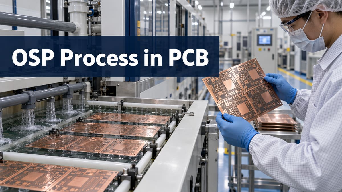
The OSP process in PCB manufacturing applies a thin organic solderability preservative directly to exposed copper after the board pattern and solder mask are complete. The film limits copper oxidation before assembly and leaves a flat pad surface for fine-pitch printing. Unlike a metallic finish, OSP is a temporary protective layer: copper preparation, coating chemistry, handling, storage and soldering history form one control chain.
Thindry can review finish selection together with pad geometry, assembly route and test/contact requirements. Send Gerber or ODB++, fabrication drawing, quantities, assembly thermal sequence, packaging needs and required acceptance tests for engineering review and quotation. Do not specify OSP only by name when shelf life, multiple heat cycles or exposed contacts are critical.
What Is the OSP Process in PCB Manufacturing?
OSP is a copper-selective organic treatment. It reacts with clean copper to form a protective film over pads and other exposed copper while generally not coating solder mask or laminate. During soldering, flux and heat remove or displace the film so solder can wet the copper.
The process is sensitive because the finish does not hide poor copper preparation. Residue, oxide, fingerprints or solder-mask contamination can prevent a uniform reaction. A board can look acceptable while local solderability has already been compromised.
How Does the OSP Process in PCB Manufacturing Work?
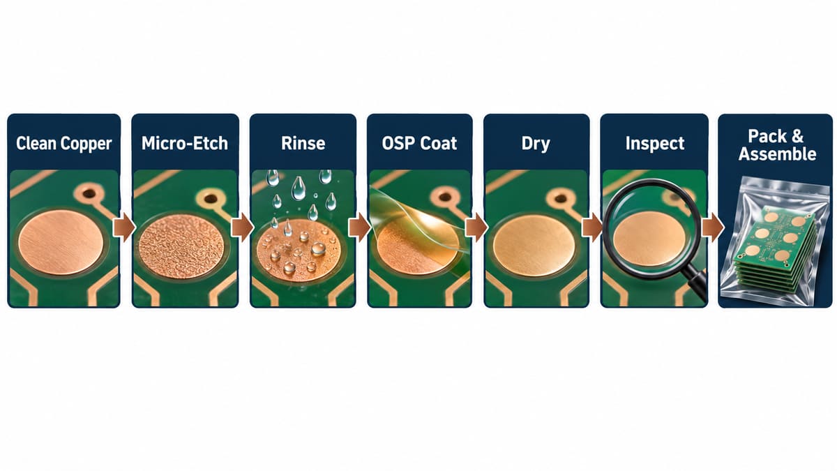
The factory sequence begins after solder mask and before final packaging. The exact chemistry and limits belong to the qualified process and purchase specification.
1. Job and Finish Requirement Review
Engineering confirms that OSP suits soldering, storage, test probing and any exposed-contact function. Edge contacts, repeated wiping or wire bonding may require another finish. The released drawing should identify OSP, applicable performance requirement and any mixed-finish areas.
2. Panel Inspection and Copper Exposure Check
Panels are checked for mask registration, residue, oxidation and damage. Solder mask on a pad cannot be corrected by the OSP bath. Defects should be resolved before coating rather than accepted under a new film.
3. Cleaning and Micro-Etching
Cleaning removes organic contamination; controlled micro-etching exposes a fresh, active copper surface. Too little preparation leaves oxide or residue, while excessive attack can change features or surface condition. Bath condition, rinse quality and copper-removal controls matter.
4. Rinsing and Surface Conditioning
Carryover from the preparation stages can contaminate the OSP bath or leave nonuniform reaction sites. Rinse-water control and prompt transfer limit re-oxidation. The surface should not be touched between preparation and coating.
5. OSP Coating
The panel contacts the controlled OSP chemistry for the qualified time and temperature. Concentration, contamination, pH where applicable, loading and agitation affect deposit formation. A named chemistry needs its own operating window; a generic internet recipe is not a production specification.
6. Final Rinse and Drying
Excess chemistry is removed and the board is dried without depositing contamination or overheating the finish. Water spots, incomplete drying or aggressive handling can shorten the useful assembly window. Drying conditions should follow the chemistry supplier’s qualified process.
7. Coating and Appearance Inspection
Visual inspection can find stains, exposed oxidation, scratches and handling damage, but appearance alone does not prove coating performance. Thickness/process checks and solderability evidence should be defined by the applicable specification and risk.
8. Electrical Test, Packaging and Release
Test strategy must account for the finish and probe contact; the sequence should avoid unnecessary damage to final pads. Clean handling and sealed protective packaging preserve the released condition. Lot identity, coating date/process record and packaging status support traceability.
9. Assembly and Rework Control
The assembler controls unpacking, floor exposure, paste/flux compatibility, thermal cycles and rework. Unsoldered OSP features can lose protection through repeated heat or abrasion. The fabrication and assembly teams should agree on the complete heat history before choosing the finish.
Which Materials and Process Inputs Control OSP Quality?
| Input | Why it matters | Evidence |
| Incoming copper surface | OSP bonds selectively to reactive copper | Pre-coat inspection and preparation control |
| Cleaner/micro-etch | Removes contamination and oxide without uncontrolled attack | Bath checks and replenishment record |
| Rinse water | Limits chemical carryover and residue | Defined water/process monitoring |
| OSP chemistry | Controls film formation and heat/storage durability | Material lot, bath status and qualified recipe |
| Packaging | Protects against moisture, contamination and abrasion | Pack method, label and release condition |
When Should You Choose OSP Instead of ENIG or HASL?
Choose by the next manufacturing and product function, not finish popularity.
| Decision | OSP fit | Review another finish when |
| Pad flatness | Strong for stencil printing and fine features | A different contact or bonding surface is required |
| Cost/process simplicity | Often attractive for controlled assembly flow | Long or uncertain storage dominates |
| Thermal history | Suitable when the qualified assembly sequence is known | Many heat/rework cycles leave unsoldered features |
| Mechanical contact | Not intended as a wear-resistant contact finish | Edge fingers, keypads or repeated probing are functional surfaces |
Compare the broader OSP versus ENIG selection separately from the process controls described here.
What Are the Main OSP Manufacturing and Assembly Failures?
| Failure sign | Possible source | Next evidence |
| Non-wetting/dewetting | Contamination, oxidation, damaged film, flux/thermal mismatch | Compare good/bad pads, lot history and solderability under defined conditions |
| Discoloration | Preparation, rinse, drying, packaging or heat exposure | Do not judge color alone; review process and performance evidence |
| Probe inconsistency | Contact strategy or coating condition | Test sequence, probe setup and affected feature map |
| Second-side solderability loss | First reflow plus delay/handling or unsuitable process window | Recorded thermal/exposure history and staged solderability trial |
How Do Design and Assembly Planning Affect OSP Reliability?
Identify every exposed copper feature and its function. A solder pad, test point, press contact and edge finger do not have the same needs. Define whether test occurs before or after finish, how many thermal cycles the board sees, and whether unsoldered copper must remain usable afterward.
Coordinate fabrication and assembly dates, packaging opening, staging and rework. Avoid bare-hand contact and uncontrolled cleaning. For upstream mask controls, review the PCB solder mask process, because contamination or misregistration left on pads cannot be repaired by OSP.
What Tests Ensure OSP Quality and Solderability?
Use complementary checks. Bath/process records show that the line operated inside its window; deposit measurement characterizes the coating; appearance finds damage; solderability testing demonstrates wetting under specified conditioning. None alone proves the entire assembly life.
- Define the governing finish and solderability specifications.
- State conditioning/aging, method, sample plan and acceptance criteria.
- Record material/bath lot and coated-board lot.
- Test after representative storage or thermal exposure when that is the risk.
- Establish reaction and containment rules for a failed result.
How Long Does the OSP Process Take?
The coating line itself is only part of lead time. Queue, pre-clean approval, chemistry condition, inspection, electrical test, packaging and any solderability report also matter. Shelf-life or assembly-window claims must be tied to the chemistry, packaging, storage and thermal sequence; do not rely on one universal number.
How Do You Choose an OSP PCB Manufacturer?
Ask whether the supplier can explain its copper-preparation controls, chemistry monitoring, coating verification, packaging and assembly limitations. Request the exact performance basis and a clear reaction plan for nonconformance. A low price and a brown-looking pad are not sufficient qualification evidence.
What Should an OSP PCB RFQ Include?
- Gerber/ODB++, drill/rout files and fabrication drawing.
- OSP requirement and applicable performance/solderability criteria.
- Board quantity, panel format and required packaging.
- Expected storage, shipment and assembly timing.
- Number and type of reflow, wave/selective and rework exposures.
- Test points, connector/contact surfaces and any mixed finishes.
- Required certificate, lot traceability and test report.
Frequently Asked Questions
Does OSP add a metal layer to copper?
No. It is an organic copper preservative, not a metallic plating stack.
What happens to OSP during soldering?
Flux and heat remove or displace the film so solder can wet the underlying copper. The exact result depends on compatible materials and process conditions.
Can OSP be used on edge connectors?
It is generally not a wear-resistant contact finish. Review a finish designed for the required mechanical and electrical contact life.
Is OSP suitable for fine-pitch components?
Its flat surface can support fine-feature printing, but pad design, stencil, paste, warpage and assembly controls still determine yield.
Can visual inspection prove OSP quality?
No. Appearance can find damage or staining but cannot replace process, deposit or solderability evidence.
Can an OSP board be baked before assembly?
Only use a bake condition supported by the board/chemistry supplier and assembly plan. Uncontrolled heat may reduce the remaining protection.
Why does a second reflow matter?
The first heat exposure can reduce protection on unsoldered features. Validate the complete thermal sequence and delay between sides.
What files are needed for quotation?
Send fabrication data, drawing, finish criteria, quantities, packaging and the planned assembly/test sequence.
Request an OSP Process Review
Send your board files, finish requirement, quantity, assembly heat sequence and solderability/test needs through the contact page. Thindry can review whether OSP matches the manufacturing, handling and contact requirements before quotation.


0 Comments