




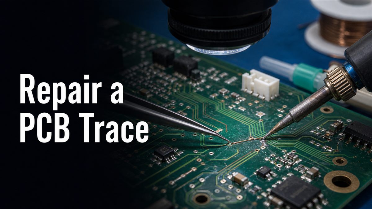
To repair a PCB trace, first confirm the trace is actually broken, clean and expose the damaged copper, bridge the open section with solder, copper tape, or a fine wire, then verify continuity, resistance, clearance, and load behavior before returning the board to service. A small signal trace may be repairable by hand, but high-current, high-voltage, impedance-controlled, buried, or safety-critical traces often need professional repair or a new PCB.
This guide explains how to judge the damage, what tools to use, how to make a practical trace repair, and how to test the result without creating a new failure point.
What is a PCB trace repair?
A PCB trace repair restores a broken copper path on a printed circuit board. The damaged trace may be open, lifted, burned, corroded, scratched, or separated from a pad or via. The repair creates a new conductive bridge so current or signal can pass through the original net again.
Common trace damage causes include mechanical scraping, overheated soldering, corrosion, liquid exposure, burned components, failed rework, connector stress, and excessive current. Before repair, identify whether the trace is only physically damaged or whether a deeper circuit fault caused it to burn.
If you need background on trace function, see what a PCB trace is.
When should you repair a PCB trace and when should you replace the board?
Repair is reasonable when the damaged trace is accessible, low-risk, and can be verified after repair. Replacement or professional review is safer when the trace carries high current, high voltage, controlled impedance, RF signals, safety functions, or disappears into inner layers.
| Condition | Repair Fit | Reason |
|---|---|---|
| Short exposed signal trace | Usually repairable | Can be bridged and tested directly |
| Small corrosion break | Often repairable | Clean copper and protect after repair |
| High-current power trace | Needs caution | Wire gauge, heat rise and fusing risk matter |
| Controlled impedance or RF trace | Usually not ideal for hand repair | Geometry changes affect signal behavior |
| Inner-layer trace | Usually not repairable by simple surface work | Damage is not accessible or easy to verify |
| Burned trace from unknown cause | Repair only after root cause is found | A shorted component may burn the repair again |
What tools do you need to repair a PCB trace?
Use tools that allow controlled, clean work. Trace repair is not just adding solder; it is restoring conductivity without shorting nearby pads or weakening the board.
- Magnifier or microscope
- Multimeter for continuity and resistance checks
- Fine-tip soldering iron
- Flux pen and suitable solder
- Isopropyl alcohol and lint-free swabs
- Sharp blade or fiberglass pen for mask removal
- Fine insulated wire, bare copper wire, or copper tape
- Tweezers and Kapton tape
- UV solder mask, epoxy, conformal coating, or repair coating
If the board already has soldering defects, compare the repair with basic soldering practices in how to solder PCB.
How do you repair a broken PCB trace step by step?
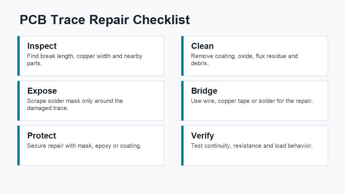
The basic repair sequence is inspect, clean, expose, bridge, secure, and verify. Work slowly; most failed repairs happen because too much solder, heat, scraping, or force is used.
- Disconnect power. Remove batteries, adapters, loads, and cables before repair.
- Inspect under magnification. Confirm the break location and check whether nearby pads, vias, or components are also damaged.
- Clean the area. Remove corrosion, dust, burnt residue, old flux, or conformal coating.
- Expose copper. Carefully scrape solder mask from both sides of the broken trace until clean copper is visible.
- Tin the copper. Apply flux and lightly tin the exposed copper with solder.
- Bridge the break. Use a short solder bridge only for very small gaps; use wire or copper tape for larger gaps.
- Secure the repair. Anchor wire with coating, epoxy, or solder mask so vibration cannot lift it.
- Inspect clearance. Check that the repair does not touch adjacent traces, vias, pads, or shield areas.
- Test continuity. Use a multimeter to confirm the repaired net is connected.
- Test function carefully. Power the board with current limiting if possible.
PCB trace repair checklist
| Check | Pass Condition |
|---|---|
| Continuity | The repaired trace connects from test point to test point. |
| Resistance | The repair has low resistance compared with expected trace behavior. |
| Clearance | No solder, wire, or copper tape touches adjacent nets. |
| Mechanical hold | The wire or copper bridge is secured and cannot lift easily. |
| Thermal behavior | The repair does not heat abnormally under load. |
| Root cause | The original reason for trace damage is understood or removed. |
How do you test a repaired PCB trace?
Testing should begin with power off. Use continuity mode to confirm the repaired trace is connected, then use resistance mode to compare the repaired path with expected circuit behavior. If the trace is near power rails, also check that the repair did not create a short to ground or to a neighboring net.
After power-off checks pass, apply power carefully. A current-limited bench supply is safer than connecting a full power source immediately. Watch input current, measure key voltage rails, and touch-test only where safe. If the repaired trace carries load current, confirm the wire or copper bridge is sized for the current and does not overheat.
For more diagnostic detail, see how to test a PCB with a multimeter.
What mistakes should you avoid during PCB trace repair?
- Repairing a burned trace before finding the short or overload that caused it.
- Using a solder blob for a long gap instead of a wire bridge.
- Scraping too much solder mask and exposing adjacent copper.
- Using wire that is too thin for a power trace.
- Leaving the repair unprotected from movement, corrosion, or vibration.
- Assuming continuity means the board is fully functional.
- Repairing RF, high-speed, or safety-critical traces without checking performance impact.
When should a repaired PCB be redesigned or remade?
A one-off trace repair may be acceptable for troubleshooting or a non-critical prototype. If the same trace fails again, the board should be redesigned or remade. Repeated failure may point to insufficient trace width, poor mechanical support, thermal stress, corrosion exposure, connector strain, or an incorrect current path.
For production boards, repair should not hide a design or manufacturing problem. If the damage came from a layout error, footprint error, assembly defect, or insufficient copper width, update the design files and request a corrected PCB. PCBTRY can review Gerber files, stackup, copper width, DFM notes, and test requirements before a remake. Send files and repair context to [email protected] for an engineering review or replacement PCB quote.
FAQs about PCB trace repair
Can a broken PCB trace be repaired?
Yes, many broken surface traces can be repaired if the damage is accessible and low risk. The repair usually uses solder, copper tape, or a fine wire bridge. Inner-layer, high-current, high-voltage, RF, or safety-critical traces need more caution.
Can I use wire to repair a PCB trace?
Yes. Fine insulated wire is often the cleanest repair for a broken signal trace or a longer damaged section. Strip and solder only the ends, then secure the wire so movement does not lift the copper pads.
Can I repair a PCB trace with only solder?
Only for a very small gap. A long solder blob is weak, can crack, and may short to nearby copper. For larger breaks, use a wire bridge or copper tape and protect the repair after testing.
How do I find a broken PCB trace?
Inspect the board under magnification and use continuity mode on a multimeter. Probe from pad to pad or via to via along the suspected net. Compare against a schematic or known-good board when possible.
Should I scrape solder mask before trace repair?
Yes, but only enough to expose clean copper on both sides of the break. Scraping too much can expose adjacent traces and increase short-circuit risk.
How do I protect a repaired PCB trace?
After testing, cover the repair with UV solder mask, epoxy, conformal coating, or another suitable insulating repair coating. This prevents corrosion, accidental shorts, and wire movement.
Can a high-current PCB trace be repaired with thin wire?
No. A high-current trace needs a repair conductor sized for the current and heat rise. Thin wire may overheat or fail. If the current is significant, calculate or verify the repair path before use.
Can a repaired trace affect signal quality?
Yes. Extra wire length, changed geometry, and added capacitance or inductance can affect high-speed, RF, clock, or impedance-controlled signals. These traces are often better redesigned or professionally evaluated.
Why did the PCB trace burn?
A burned trace may be caused by a short circuit, overload, wrong component, reversed polarity, poor copper width, or damaged downstream part. Find the cause before repairing, or the new bridge may fail again.
When should I order a new PCB instead of repairing it?
Order a new PCB when the trace is safety-critical, high current, hidden in an inner layer, repeatedly failing, or tied to a design/manufacturing error. A repair may help diagnosis, but production boards should use corrected design data.


