




Have you ever cracked open an old remote control or a broken pair of headphones? If you have, you probably saw a thin, flat board inside — usually green, sometimes blue or red, with tiny metal parts soldered onto it.
That board is a PCB. And once you understand what it does, you’ll never look at any electronic device the same way again.
This guide explains how a PCB board works. We’ll walk through the parts, the process, and a real example you can try at home.
What Is a PCB, Really?
PCB stands for Printed Circuit Board. In the simplest terms, it’s a flat board that connects electronic components together so they can talk to each other.
Think of it this way. Imagine you have a few hundred Lego bricks, and you want to build something that actually works — like a little robot. You need something to hold all those bricks in the right position, right? That’s what a PCB does for electronic parts. It holds them in place and wires them together, so electricity can flow exactly where it needs to go.
Without a PCB, you’d have to connect every component with individual wires. For a simple flashlight, that might work. But for a smartphone with over a thousand components? Forget it.
So the PCB solves a huge problem: it takes a messy web of connections and turns them into a neat, flat, manufactured board that can be mass-produced.
The Basic Parts of a PCB
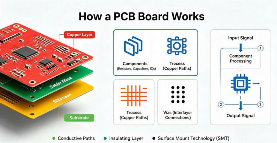
A PCB isn’t just one thing. It’s made up of several layers and features, each with a specific job. Let’s break them down.
| Part | What It Is | Everyday Analogy |
|---|---|---|
| Substrate (Base) | The core material of the board, usually fiberglass | The ground a city is built on |
| Copper Traces | Thin copper pathways etched onto the board | The roads that connect buildings |
| Pads | Small copper areas where components get soldered | Parking spots at each building |
| Vias | tiny holes that connect copper layers together | Overpasses or tunnels between roads on different levels |
| Silkscreen | White (or colored) labels and markings printed on the board | Street signs and labels |
| Solder Mask | The green (or other color) coating on top of the copper | The paint on a road that keeps it from wearing out |
| Components | The actual electronic parts: resistors, capacitors, chips, etc. | The buildings, shops, and houses in the city |
When you look at a PCB, most of what you see is the solder mask (the green stuff) and the silkscreen (the white writing). The copper traces are hiding underneath, doing all the real work.
How a PCB Actually Works: 5 Steps
Now let’s get to the main question. How does a PCB actually do its job? Here’s the process in five plain steps.
Step 1: Power Comes In
Every PCB needs power. Electricity enters the board through a connector — could be a USB port, a battery terminal, or a power jack. Think of this as the highway on-ramp. Without it, nothing moves.
Step 2: Current Flows Through the Traces
Once power enters, it travels along the copper traces. These traces are like roads laid out on a map. They’re designed to carry electricity from one point to another — from the power source to the components that need it.
Here’s the key: the copper traces don’t carry electricity randomly. They follow a specific path that the PCB designer planned. Every turn, every branch, every connection is intentional.
Step 3: Components Do Their Jobs
As electricity reaches each component, that component does what it’s designed to do:
- Resistors slow down the current (like a speed bump on a road)
- Capacitors store and release energy (like a small battery that charges and discharges quickly)
- Diodes let current flow in only one direction (like a one-way street)
- Integrated circuits (chips) process information (the “brain” of the board)
Step 4: Signals Pass Between Components
It’s not just about power. Components also send signals to each other — tiny electrical pulses that carry information. A button press tells a chip “something happened.” The chip then sends a signal to an LED, a motor, or a wireless antenna to respond.
All of this happens through the copper traces and vias. The PCB is both the power grid and the communication network.
Step 5: The Device Does Something You Can See
After all the internal processing, the device produces a result: a screen lights up, a speaker plays sound, a Wi-Fi signal gets sent. The PCB made it all happen behind the scenes.
A Real Example: What Happens When You Press a Button on a Remote Control
Let’s make this concrete. Here’s what happens inside a typical TV remote when you press the power button:
- You press the button. Underneath the rubber pad, a small metal dome collapses and touches a copper pad on the PCB. This completes a circuit.
- The PCB sends a signal to the chip. Electricity flows from the pad through a copper trace to the main integrated circuit (the little black square in the center of the board).
- The chip processes the signal. It knows which button you pressed because each button is wired to a different input pin on the chip. The chip looks up the corresponding command code.
- The chip tells the infrared LED to fire. A signal goes out through another copper trace to the LED at the front of the remote. The LED blinks in a pattern that represents the “power on” command.
- Your TV receives the signal and turns on. Done.
All of this happens in a fraction of a second. And the PCB is the stage where every one of those steps takes place.
Try this: pull apart an old remote and look at the board. You’ll see the copper pads under each button, the chip in the middle, and the LED at the front — all connected by thin copper lines. That’s the PCB doing its job.
Single-Layer vs. Multi-Layer PCBs
Not all PCBs are built the same. Some have copper on just one side. Others have copper sandwiched between multiple layers — sometimes 4, 8, or even dozens.
Single-layer PCBs have copper traces on one side of the board. They’re cheap, simple, and good enough for basic devices. Think of your TV remote, a simple LED light circuit, or a basic calculator.
Double-layer PCBs have copper on both sides. This gives designers more room to route traces. Most consumer electronics use at least double-layer boards.
Multi-layer PCBs stack several copper layers inside the board, separated by insulating material. This is how you fit thousands of connections into a tiny space. Your smartphone, laptop, and smartwatch all use multi-layer PCBs — often 6 to 12 layers deep.
Here’s a quick comparison:
| Type | Copper Layers | Typical Use | Cost |
|---|---|---|---|
| Single-layer | 1 | Remote controls, simple toys, LED circuits | Low |
| Double-layer | 2 | Power supplies, USB hubs, industrial controls | Moderate |
| Multi-layer (4–8) | 4 to 8 | Smartphones, tablets, routers | Higher |
| High-density (10+) | 10 or more | Laptops, servers, medical devices, aerospace | Highest |
The more layers a PCB has, the more connections it can support in a smaller area. But more layers also mean more manufacturing complexity and higher cost. That’s why a remote control uses a single-layer board while a MacBook uses a 10-layer board.
Why PCBs Are Green (and Other Colors You Might See)
You’ve probably noticed that most PCBs are green. Why are most PCBs green?
The answer is simple: it’s the color of the solder mask. The solder mask is a thin protective coating applied over the copper traces. Its job is to prevent accidental short circuits, protect the copper from dust and moisture, and make soldering easier during manufacturing.
Green became the standard because it’s the easiest color for manufacturers to work with. The human eye picks up green well, which makes it easier for quality inspectors to spot defects on the board. It’s also the cheapest pigment to produce at scale.
But green isn’t the only option. You’ll find PCBs in plenty of other colors:
- Blue — Commonly used by OSH Park and some open-source hardware projects. Looks clean and modern.
- Red — Often seen on Arduino boards and dev kits. Stands out visually.
- Black — Popular in premium consumer electronics. Looks sleek but makes trace inspection harder (black absorbs light).
- White — Frequently used for LED boards because it reflects light well.
- Yellow/Orange — Less common, sometimes used for flexibility boards or specific branding.
At the end of the day, the color doesn’t affect how the PCB works. A green board and a red board with the same design will perform identically. Color is about manufacturing practicality and aesthetics — nothing more.
Common Misconceptions About PCBs
After years of working with PCBs, I’ve noticed a few misconceptions that come up again and again. Let’s clear them up.
“The PCB is the chip.” No. The chip (integrated circuit) is just one component on the PCB. The PCB itself is the board — the platform that holds and connects all the components, including the chip.
“A PCB is just a piece of plastic with metal on it.” It’s more than that. The layout of the copper traces is a carefully engineered design. Changing the width of a trace, the distance between two traces, or the placement of a via can affect whether a device works reliably or fails. PCB design is a real engineering discipline.
“More copper always means better performance.” Not necessarily. Extra copper adds weight and cost. Sometimes you want thin traces for signal integrity. Sometimes you need wide traces for high-current paths. It’s about balance, not excess.
“Any PCB can be replaced by a breadboard.” Breadboards are great for prototyping, but they can’t handle high frequencies, high currents, or miniaturized designs. Once you move from “testing” to “shipping a product,” you need a real PCB.
Why PCB Design Matters
A PCB isn’t just a container for components. The way it’s designed directly affects how well a product performs.
Here are a few things that depend on PCB design:
- Signal quality — If traces are poorly routed, signals can get distorted. This shows up as glitches, noise, or data errors.
- Power stability — Bad power routing causes voltage drops. Your device might reboot randomly or behave unpredictably.
- Heat management — Components that run hot need copper planes to spread heat. Without them, components can overheat and fail.
- Manufacturing yield — A poorly designed PCB is harder to manufacture, which means more defects and higher cost.
This is why PCB design isn’t just about making connections. It’s about making the right connections in the right way.
How to See a PCB in Real Life
The best way to understand a PCB is to look at one yourself. Here’s what you can do:
- Find an old remote control, a broken pair of earbuds, or a retired router. Most households have at least one old electronic device sitting in a drawer.
- Open it up. You might need a small screwdriver. Be careful not to touch any capacitors if the device was recently plugged in — they can hold a charge.
- Look for the board inside. Identify the parts: the copper traces, the chip, the button pads, the LED, the battery contacts.
- Compare what you see to this article. See if you can trace the path from the power source to the components. Find the vias connecting different layers. Read the silkscreen labels.
You’ll be surprised how much more everything makes sense once you can see it in your hands.
Summary: A PCB in One Sentence
If you remember nothing else from this article, remember this:
A PCB is the road system that tells electricity where to go and connects every component into a working whole.
It’s not a chip. It’s not a piece of plastic. It’s the invisible infrastructure behind every electronic device you use — from your toothbrush to your car’s dashboard to the phone you’re reading this on.
Now that you know how a PCB works, here’s a challenge: find one, hold it in your hand, and trace the copper paths with your eyes. Follow the road from the power input to the biggest chip. You’ll be surprised how much sense it suddenly makes.
Once you see the road map, you can’t unsee it.



0 Comments