




Introduction
FR4 glass-reinforced epoxy laminate is, by a wide margin, the most popular base material in PCB manufacturing. It’s made by impregnating glass fiber cloth (types like 7628, 2116, or 1080) with epoxy resin and curing it under heat and pressure. The result is a material with solid insulation, decent mechanical strength, and excellent processability.
But here’s the thing most engineers don’t think about until something goes wrong: substrate thickness.
The thickness you pick doesn’t just determine how thick your final board is. It ripples through impedance control, thermal management, mechanical reliability, and ultimately, how much your board costs to produce. Pick wrong, and you might find yourself fighting warpage on the reflow line, missing impedance targets on a high-speed design, or watching solder joints crack in the field.
This article breaks down FR4 thickness from the ground up — starting with standard thickness categories, then walking through how thickness affects each of those four critical areas, with real-world examples and a practical selection guide you can actually use.
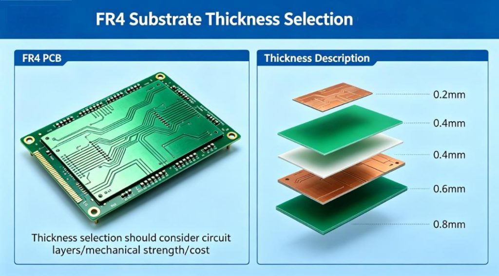
Base Material Thickness vs. Finished Board Thickness
Before we go any further, let’s clear up a confusion that trips people up regularly: substrate thickness is not the same as finished board thickness.
- Substrate thickness refers to the dielectric layer — the fiberglass cloth plus resin — in a prepreg sheet or core laminate. This is the value you plug into impedance calculators.
- Finished board thickness = substrate thickness + copper foil thickness (for all layers combined) + solder mask layers + surface finish (ENIG, OSP, etc.).
A board marked 1.6 mm on a spec sheet typically has a dielectric portion of around 1.45 mm, with the remaining thickness coming from copper (~70 µm total) and surface treatments.
So when you’re talking to your PCB fabricator, be specific: do you mean finished board thickness or substrate thickness? Getting this wrong can throw your entire stackup and impedance calculations off.
Standard FR4 Thickness Categories
Before diving into performance implications, it helps to have a mental map of the thickness landscape. Here’s what the industry typically works with:
| Finished Board Thickness (mm) | Typical Use Cases |
|---|---|
| 0.2 – 0.4 | Rigid-flex zones, micro camera modules, wearable internal flex reinforcement |
| 0.6 – 0.8 | Ultra-thin consumer electronics (TWS earbuds, smart rings), rigid sections of rigid-flex |
| 1.0 – 1.2 | IoT modules, non-high-speed control boards, space-constrained consumer products |
| 1.6 | The industry default — consumer electronics, industrial control, telecom, basic power supplies |
| 2.0 – 2.4 | High-power power supplies, automotive (ECUs, BMS), applications needing serious mechanical strength |
| 2.4 – 3.2+ | Data center motherboards, high-power inverters, mil-spec structural PCBs |
Something like 70% of all PCBs manufactured worldwide are 1.6 mm thick. It strikes the best balance between cost, process yield, and general-purpose performance. But plenty of applications need to go thinner — or thicker.
How Thickness Affects Impedance Control
The Basic Physics
The characteristic impedance of a microstrip line on a PCB is approximated by:
Z0=εr+1.4187ln(0.8w+t5.98h)
where h is the dielectric thickness (distance between the conductor and reference plane), w is trace width, t is copper thickness, and is the relative permittivity of the dielectric.
The takeaway: all else being equal, a thicker dielectric means higher impedance. If your substrate thickness drifts from the design value — whether from manufacturing tolerance or a material change — your impedance moves with it. On high-speed lines, even a few ohms of deviation can cause reflections, timing errors, and EMI headaches.
What This Means in Practice
For high-speed signals — DDR4/DDR5 data lines, USB 3.x, HDMI 2.1, 100G Ethernet — the target impedance is typically 50 Ω single-ended or 100 Ω differential. Achieving this requires balancing several variables:
- Trace width w: Limited by your fab’s minimum feature capability
- Copper thickness t: Driven by current-carrying requirements
- Dielectric thickness h: This is the substrate thickness — directly selectable
When the overall board thickness is constrained (say, by a slim product enclosure), you’re forced into thinner dielectrics and narrower traces to hit impedance targets. That drives up copper losses and manufacturing difficulty. On the flip side, when you have board thickness to work with, you can use wider traces, lower DC losses, and get better yields.
Practical advice: Don’t wait until layout is done to think about impedance. Run a quick stackup and impedance estimation early in the project using tools like Polar Si9000. Submit your target impedance, target finished thickness, and acceptable trace width range to your PCB supplier for review.
How Thickness Affects Thermal Performance
FR4 Is a Poor Thermal Conductor — And That’s Okay (If You Know What You’re Doing)
Let’s be blunt: FR4’s thermal conductivity is roughly 0.3 W/m·K. That’s terrible compared to aluminum substrates (1–3 W/m·K) or ceramics (20–200 W/m·K). Cranking up the FR4 thickness to “help with heat dissipation” is largely a waste of copper and money. Heat moves painfully slowly through the resin-fiberglass matrix.
Where Thickness Still Matters for Heat
That said, board thickness does shape the thermal picture indirectly:
- Thinner boards put heat sources closer to the back-side copper plane, which can be tied to an external heatsink or metal housing. Short thermal path = lower thermal resistance, assuming you’ve designed the thermal interface properly. This is the go-to strategy for LED drivers, portable chargers, and compact power modules.
- Thicker boards have more thermal mass, which can buffer transient power spikes. They also tend to come with heavier copper (2 oz, 3 oz), which improves lateral heat spreading. But the long vertical thermal path through FR4 works against you.
In practice, copper weight, copper area, and thermal via density matter far more than board thickness for heat dissipation. If you’re dealing with high power density, look at:
- Using multilayer stackups with internal ground/power planes as thermal spreaders
- Placing dense arrays of thermal vias under hot components (MOSFETs, power ICs) to route heat to the back-side copper pour
- Considering high-thermal-conductivity FR4 (up to ~1.0 W/m·K) or switching to a metal-core substrate when FR4 simply can’t cut it
How Thickness Affects Mechanical Reliability
Stiffness Scales with the Cube of Thickness
The relationship between board thickness and bending resistance isn’t linear — it’s cubic. The second moment of area I is:
I=12bh3
where b is the board width. Double the thickness, and you get roughly eight times the stiffness. That’s why a 0.6 mm board buckles under stresses that a 1.6 mm board shrugs off without blinking.
Two Stories from the Real World
Case 1: Battery Management System in a New Energy Vehicle
A Tier 1 automotive supplier was developing a slave controller board for an EV battery management system (BMS). The board measured 200 mm × 150 mm and carried several large aluminum electrolytic capacitors, power relays, and multiple connectors interfacing with cell modules. The initial design used 1.6 mm FR4 with 1 oz copper.
During vibration testing per ISO 16750-3, solder joints near the connector area began showing micro-cracks. The root cause was twofold: the mechanical stress from repeated connector insertion/extraction combined with long-term vehicle vibration was causing the board to flex excessively. At 1.6 mm, the board simply didn’t have enough stiffness to survive the mechanical demands of an automotive environment over the product’s lifetime.
The fix: Increase the board to 2.0 mm finished thickness with 2 oz outer copper. Add reinforced stiffener structures along the board edges. Re-test passed with a 3× improvement in solder joint lifespan, clearing the automotive reliability standard with margin.
The lesson: For automotive PCBs with large board areas and dense connectors, anything below 2.0 mm is asking for trouble unless you add external stiffeners. BMS and other safety-critical automotive boards should generally start at 2.0 mm as a baseline.
Case 2: Smartwatch Main Logic Board
A major wearable brand was pushing the limits of miniaturization for their flagship smartwatch. The main control board had to fit within extreme Z-height constraints, driving the design to 0.6 mm finished thickness using 0.4 mm substrate with fine-line processing. The first problem that showed up during production? Severe warpage during lead-free reflow soldering. BGA pads weren’t making proper contact, and initial yield was a painful 70%.
The fix took three steps:
- Stackup symmetry: Rebalanced the prepreg layers so the top and bottom halves of the stackup mirrored each other symmetrically. Asymmetric stackups are the number one cause of thermal warpage.
- Copper balancing: Added sacrificial copper patterns (copper thieving) on under-populated layers to equalize copper density across the board.
- Reflow process tuning: Adjusted the oven profile and board orientation to minimize thermal gradient stress.
Post-fix warpage dropped below 0.5% (the industry guideline is typically ≤0.75%), and production yield climbed to over 95%.
The lesson: For ultra-thin boards (≤0.6 mm), stackup symmetry and copper balance matter more than the thickness number itself. Engage your SMT supplier early — the reflow process window for thin boards is narrow, and you don’t want to discover this after the board is manufactured.
Practical Rules of Thumb
- Below 0.8 mm: Warpage control becomes critical. Pay close attention to copper distribution, stackup symmetry, and reflow process compatibility, especially for boards with large BGAs.
- Above 2.0 mm: Drill depth and plating uniformity become concerns. High aspect ratio through-holes need special attention — confirm your fab’s capability before finalizing the design.
- High-reliability sectors (automotive, aerospace, medical): Default to 1.6 mm or thicker, and supplement with stiffeners or metal reinforcement where needed.
How Thickness Affects Cost
Cost is the constraint that brings every design back to earth. Here’s how thickness maps to cost:
| Thickness Range | Material Cost | Processing Difficulty | Yield | Overall Cost Impact |
|---|---|---|---|---|
| ≤0.4 mm (ultra-thin) | High (specialty cloth) | High (warpage, depaneling) | Low | Highest |
| 0.6 – 1.2 mm | Normal | Moderate | Moderate | Moderate |
| 1.6 mm (standard) | Lowest | Low | Highest | Lowest |
| 2.0 – 2.4 mm | Slightly higher | Moderate (deep drilling) | Moderate | Moderate-high |
| ≥3.0 mm | Much higher | High (heavy copper build-up) | Low | Highest |
A few ways to keep costs in check:
- Default to 1.6 mm when possible. It’s the most common stock thickness across the industry. No special procurement, no extended lead times, best pricing.
- Don’t over-engineer the thickness. If the board is a simple controller with no high-speed signals, no vibration exposure, and no high current, 1.6 mm is almost always sufficient. Thinner or thicker just adds cost for no real benefit.
- Standardize across product lines. Using the same board thickness across multiple products lets you consolidate material purchases and simplify production scheduling.
- Confirm tolerances during prototyping. Typical thickness tolerance is ±10%. For designs where stackup thickness is critical (metal-enclosed assemblies, controlled impedance), specify ±5% — there’s a small sorting surcharge, but it saves you from assembly failures later.
Common Misconceptions About Thickness Selection
| Myth | Reality |
|---|---|
| Thicker boards are always more stable | Stability depends on copper weight, Tg value, and stackup symmetry too. Blindly adding thickness can create drilling problems. |
| Thinner boards are inherently better for RF/high-frequency | High-frequency performance is driven more by Dk (dielectric constant) and Df (dissipation factor) than by thickness. Thinner dielectrics do reduce dielectric loss path length, but material selection matters more. |
| Any FR4 works for high-speed signals | Standard FR4 has a Df around 0.02, which is too lossy for signals above ~10 Gbps. Use low-loss variants (e.g., IT-180G, Megtron 6) for serious high-speed work. |
| Finished board thickness equals substrate thickness | Finished thickness includes copper layers, solder mask, and surface finish. The actual dielectric is typically 0.05–0.15 mm thinner. |
| Thickness tolerance doesn’t matter | On impedance-critical high-speed boards, a ±10% thickness variation can push impedance outside the ±5% spec window. Tight tolerances are worth the cost. |
Quick Reference: Thickness Selection by Application
| Application | Recommended Thickness (mm) | Key Considerations |
|---|---|---|
| Wearables (fitness bands, TWS earbuds) | 0.4 – 0.8 | Extreme space constraints, warpage during reflow |
| Consumer electronics (phones, tablets) | 0.8 – 1.2 | Impedance control, stackup symmetry |
| General-purpose control boards / IoT | 1.0 – 1.6 | Cost-driven, broad applicability |
| Industrial control / instrumentation | 1.6 – 2.0 | Mechanical strength, connector reliability |
| NEV automotive (BMS, VCU) | 1.6 – 2.4 | Vibration, high current, safety-critical reliability |
| Telecom / servers (high-speed) | 1.6 – 2.4 | Stackup design, impedance, material selection |
| Power supplies / high-current equipment | 2.0 – 3.2 | Heavy copper, thermal management, mechanical strength |
| Medical electronics (non-implantable) | 1.2 – 2.0 | Reliability, certification requirements |
A Practical Checklist for Thickness Selection
- Rank your priorities: Electrical performance (impedance) → mechanical reliability → thermal management → cost. (Adjust the order to fit your project.)
- Run impedance and stackup calculations early, using your target thickness to check whether your trace widths are achievable.
- Confirm manufacturable thickness with your PCB supplier. Ultra-thin and ultra-thick boards require special processes — not every fab can handle them.
- Reference IPC-4101 for FR4 grade definitions and associated thickness specifications.
- Prototype and measure: First-article boards must be tested for actual thickness, impedance, and warpage.
- Build an internal thickness standard for your organization. Repeating the same thickness research across projects wastes time and money.
Final Thought
FR4 substrate thickness isn’t an isolated design parameter. One end connects to impedance and signal integrity. The other end connects to mechanical strength and thermal behavior. And pulling both ends is cost and manufacturability.
In the rush to meet deadlines, it’s tempting to just default to 1.6 mm because “that’s what everyone uses.” For general-purpose boards, that’s fine. But in high-speed telecom, automotive power electronics, or space-constrained wearables, that reflex can come back to haunt you during validation — or worse, in the field.
The best approach is to treat thickness as a system-level decision from day one. Iterate it alongside your electrical, thermal, and mechanical design, and keep your fabricator’s capabilities in the loop. There’s no universally correct thickness — only the right thickness for your specific product.
If you’re in the middle of stackup design right now, or if you’re wrestling with impedance targets, warpage issues, or thermal challenges on a specific board, our engineering team is happy to help. We offer free stackup consulting and prototype validation support — reach out and let’s figure it out together.



0 Comments