




How to Fix Solder Balling Issues in Selective Soldering: Practical Troubleshooting from the Process Side
Anyone who has worked with selective soldering for a while has probably seen this problem: small solder balls showing up around the solder joints.
Sometimes there are only a few tiny dots, visible mainly under magnification. Sometimes they are scattered across an entire soldering area. Solder balls may not look as serious as bridging, and they may not fail functional testing immediately like an open joint. But they can still become a real quality concern. In automotive electronics, industrial control boards, power modules, and communication products, any loose solder ball that may move, detach, or create a short circuit cannot be treated as a simple cosmetic issue.
In selective soldering, this defect is usually called solder balling or solder beads. The root cause is rarely just one single parameter. In many real production cases, flux application, preheating, solder wave behavior, nozzle condition, PCB design, board moisture, and material condition all interact with each other. The final symptom is simply a few small shiny solder balls near the joint.
That is why the first question should not be, “What solder temperature should I set?” A better approach is to look at where the solder balls appear, then decide whether the issue is more likely related to materials, equipment, process parameters, or PCB design.
The following points are written from a shop-floor troubleshooting perspective. The focus is not on theory for the sake of theory, but on how a process engineer would actually check and improve the process.
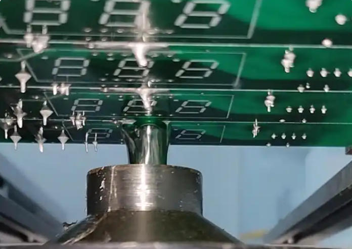
First Check Whether the Solder Balls Are Random or Location-Specific
When solder balls appear, do not start changing parameters right away. The first step is to observe their distribution.
If the solder balls are random, appearing in different areas from board to board, the first things to check are usually:
- unstable or excessive flux spraying;
- insufficient or fluctuating preheating;
- contaminated solder nozzle;
- excessive dross or oxidation in the solder pot;
- PCB moisture or unstable surface condition;
- unstable nitrogen protection.
If the solder balls always appear around the same connector, the same pin row, or the same pad area, then the priority should shift to:
- pad design and solder mask layout;
- local thermal imbalance caused by large copper areas;
- nozzle travel path or soldering direction;
- component layout that limits nozzle access;
- excessive dwell time or repeated heating at that position.
This distinction matters. Random defects and fixed-location defects usually come from different sources. One common mistake is to keep adjusting flux for a fixed design-related problem, or to keep reviewing Gerber files when the real issue is unstable spraying or poor nozzle maintenance.
Excessive or Uneven Flux Application: A Common Starting Point
In selective soldering, more flux does not always mean better soldering. Flux removes oxides and supports wetting, but if too much flux is applied, or if it accumulates in certain areas, the solvent and volatile components can boil rapidly when they reach the hot solder wave. This can disturb the molten solder and carry small solder particles away from the joint, forming solder balls.
A typical sign is that the solder joint still wets reasonably well, but small solder balls appear on the surrounding solder mask. In some cases, the board also shows heavy residues, sticky areas, or local whitening.
Shop-Floor Case
On one industrial control board, small solder balls appeared randomly around a connector after selective soldering. The production team first reduced the solder temperature from 285°C to 275°C. The solder balls decreased slightly, but some joints started to show poor wetting. Later, a glass plate test was used to check the flux spray pattern. It showed clear overlapping at the path corner, which caused local flux over-application.
Root Cause
The main problem was not an excessively high solder temperature. It was local flux accumulation. Lowering the solder temperature reduced spattering a little, but it also narrowed the wetting window and introduced a new risk of insufficient soldering.
Corrective Actions
- Use a glass plate, test paper, or weight measurement to confirm the actual flux amount.
- Check whether the spray nozzle is clogged, misaligned, or producing poor atomization.
- Optimize the spray path to avoid overlapping at corners or dwell points.
- Reduce spray pulse time or spray pressure carefully, while still ensuring full pad coverage.
- Include flux spray verification in first-article inspection, instead of relying only on program settings.
As a practical rule, if solder balls are random and flux residue also looks inconsistent, flux application should be one of the first items to investigate.
Insufficient Preheating: The Flux Has Not Had Enough Time to Work
Insufficient preheating is another frequent cause of solder balling in selective soldering. It creates two main problems.
First, the solvent in the flux does not evaporate sufficiently before entering the soldering zone. Once it touches the solder wave, it boils suddenly and disturbs the molten solder. Second, the PCB, pads, and leads are still too cold, so solder wetting is slower and less stable when the nozzle moves away.
This problem is especially common on thick boards, heavy copper boards, and power boards. The temperature shown on the machine is not always the real temperature at the defect location.
Shop-Floor Case
A heavy copper power board repeatedly showed solder balls around a high-current connector. At first, the team suspected oxidized connector leads and changed to another material lot, but the problem remained. Thermocouples were then attached near the connector solder joints. The measured temperature before solder contact was much lower than in other areas. The local copper area around the connector was absorbing too much heat.
Root Cause
The actual temperature at the joint area was not high enough. Flux evaporation and activation were incomplete. When the board entered the solder wave, the remaining solvent boiled quickly and caused spattering. At the same time, the colder pads reduced wetting stability and made solder balling more likely.
Corrective Actions
- Measure the real board temperature near the defect area using thermocouples.
- Increase preheating power or extend preheating time where appropriate.
- Create separate soldering programs for thick boards and heavy copper designs.
- Check temperature differences across the board, especially near large copper areas, connectors, and shielding parts.
- After changing preheat settings, verify both solder joint wetting and flux residue condition.
Do not rely only on the equipment setpoint. Many selective soldering problems are only understood after measuring the real board temperature.
Over-Aggressive Preheating: Flux Can Be Used Up Too Early
Too little preheat causes problems, but too much preheat can also cause solder balls.
If the heating rate is too fast, or if local infrared heating is too strong, the flux may evaporate too early or lose activity before the joint reaches the solder wave. The board temperature may look acceptable, but when the solder finally contacts the pad and lead, there may not be enough active flux left to support stable wetting.
This type of issue is often seen after changing to a new machine, modifying the preheating module, or introducing a new flux.
Shop-Floor Case
After one consumer control board was transferred to a new selective soldering machine, solder balls increased suddenly. The process team had copied most parameters from the old machine. However, the new machine had more efficient infrared preheating. Actual measurement showed that the board was heating much faster, and some areas of flux were already too dry before solder contact.
Root Cause
Preheating is not simply about making the board hot. Flux needs to evaporate and activate within a suitable temperature window before entering the soldering zone. If it dries out too early, wetting becomes unstable, and the solder may shrink into small balls along the pad edge or on the solder mask.
Corrective Actions
- Re-measure the actual heating profile instead of copying parameters from the previous machine.
- Reduce preheating power or adjust conveyor speed if the heating rate is too aggressive.
- Avoid direct local hot spots on the fluxed soldering area.
- Judge the result by both solder joint appearance and flux residue condition.
- Confirm the recommended preheat window with the flux supplier when necessary.
A single temperature value is not enough. Heating rate, dwell time, and temperature uniformity all need to be considered.
Excessive Solder Wave Height or Dwell Time: Less Insufficient Fill, More Solder Balls
A common reaction to insufficient solder is to increase the solder wave height. If that does not work, the next step is often to increase dwell time.
This may reduce insufficient solder in the short term. But if the settings become too aggressive, the solder wave can over-wash the pads and nearby solder mask. When the nozzle leaves the joint, the molten solder may be pulled away instead of separating cleanly. Solder balls, bridging, and solder peaks may then appear together.
Shop-Floor Case
One production line increased the solder wave height and extended dwell time to solve insufficient solder on a connector. The insufficient solder issue improved, but solder balls started to appear around the joints, and a few locations showed slight bridging. Slow-motion video showed obvious solder dragging when the nozzle moved away from the joint.
Root Cause
The original insufficient solder may have been caused by preheating, flux coverage, or local thermal mass, not by lack of solder wave contact. Increasing wave height and dwell time only forced more solder onto the joint, but also created spattering and solder balling.
Corrective Actions
- Set the solder wave height to the lowest stable level that still provides proper wetting.
- Remove unnecessary dwell time.
- Review the nozzle exit path and angle.
- For insufficient solder, check preheating and flux coverage before increasing wave height.
- Use process video to observe the exact moment when the nozzle contacts and leaves the joint.
A good solder joint should be formed by wetting, not by forcing solder onto the pad with an aggressive wave.
Nozzle Contamination and Solder Pot Oxidation: If It Gets Worse During the Shift, Check Maintenance First
If first-article boards look good in the morning but solder balls increase after several hours of production, the nozzle and solder pot condition should be checked early.
Oxides, residue, or wear around the nozzle edge can disturb the solder wave shape. Once the wave becomes unstable, molten solder is more likely to splash or separate unevenly. Excessive dross in the solder pot may also be carried into the soldering area and create granular residues or solder balls.
Shop-Floor Case
On one automotive electronics product, the first boards of the shift were acceptable, but solder balls increased in the afternoon. The program settings and flux material had not changed. After stopping the machine, the team found oxide buildup around the nozzle edge, and the solder wave looked less compact than it had in the morning. After cleaning the nozzle and removing dross from the solder pot surface, the defect rate dropped noticeably.
Root Cause
This was not a sudden parameter issue. It was equipment condition drifting during production. A dirty nozzle damaged the wave stability, while additional oxidation reduced solder flow quality.
Corrective Actions
- Define a fixed nozzle cleaning interval instead of waiting for defects to appear.
- Check the solder wave shape every shift for shaking, spreading, or spattering.
- Remove dross from the solder pot surface regularly.
- Check pump speed, solder level, and nozzle installation condition.
- Add mid-shift inspection for long continuous production runs.
If solder balls increase as production time goes on, do not rush to adjust solder temperature. Equipment condition is often the better place to start.
PCB Moisture or Surface Contamination: Batch-Related Problems Need Material Tracing
Some solder balling problems are not caused by process settings, but by unstable PCB condition.
If a PCB absorbs moisture, water can escape quickly from plated holes, solder mask edges, or small voids in the laminate during soldering. This can disturb the molten solder and produce small solder balls. Surface contamination such as fingerprints, oil, oxidation, cleaning residue, or other contaminants can also reduce wetting and make solder shrink into small beads.
This type of issue often appears as a batch-related abnormality: the same machine and same program worked well on the previous lot, but the next PCB lot suddenly shows more solder balls.
Shop-Floor Case
During a rainy season, one PCB lot showed a clear increase in solder balls after selective soldering. The same program had run normally on the previous lot. After tracing the material history, the team found that this PCB lot had been left open in the workshop for too long, and the local humidity control had not been stable. After baking a small sample batch before soldering, solder balling was significantly reduced.
Root Cause
Moisture in the PCB released vapor during high-temperature soldering, causing small solder disturbances. Surface contamination or oxidation also reduced wetting consistency, making solder balling more likely.
Corrective Actions
- Control PCB exposure time after opening the package.
- Run a baking verification for PCBs with long storage time or damaged packaging.
- Maintain dry packaging and FIFO material control.
- Avoid touching soldering areas with bare hands.
- For repeated batch issues, check ionic contamination, surface cleanliness, or solderability.
It is not good practice to blame “dirty boards” without evidence. But if the defect clearly follows a material lot, PCB storage and incoming condition must be reviewed.
Solder Mask and Pad Layout: Fixed-Location Solder Balls Are Often Not Fully Solved by Tuning
If solder balls always appear near the same few joints, and changes to flux, preheating, and wave height only help slightly, the PCB design should be reviewed seriously.
Selective soldering is sensitive to nozzle access, pad openings, solder mask web width, and thermal balance. Narrow solder mask dams, oversized exposed copper, and tight pad spacing all increase the risk of solder attachment or overflow outside the intended joint area.
Another common case is thermal imbalance within the same pin row. One pin may connect to a large copper area, while the neighboring pins connect only to thin traces. To get enough wetting on the high-thermal-mass pin, the process may need stronger heat input. But the low-thermal-mass pins nearby may then become overheated and start showing solder balls or solder overflow.
Shop-Floor Case
A connector area repeatedly showed solder balls around the same two or three pins. Adjusting flux, preheat, and wave height only provided temporary improvement. When the Gerber data was reviewed, the solder mask dam in that area was found to be narrow, and one pin was connected to a large copper plane, creating much higher thermal mass than the adjacent pins.
Root Cause
This was a narrow process window caused by design. The high-thermal-mass pin needed more heat, while the surrounding low-thermal-mass pins could not tolerate the stronger process settings. For fixed-location solder balls, PCB design factors should move higher on the checklist.
Corrective Actions
- Optimize pad size and solder mask openings.
- Increase solder mask dam width and reduce unnecessary exposed copper.
- Add thermal relief for large copper connections where appropriate.
- Confirm nozzle accessibility and soldering direction during the design stage.
- If the design cannot be changed, create local soldering parameters for that area.
In mass production, process tuning may only widen the margin. The real fix often requires a PCB design revision in the next build.
Insufficient Nitrogen Protection: Check It When Joints Look Dull and Oxidation Increases
Selective soldering often uses nitrogen to reduce oxidation around the solder wave. Nitrogen protection may not directly create solder balls, but insufficient protection increases wave oxidation, reduces solder flow, and makes wetting less stable.
Typical signs include dull solder joints, more oxide residue, a less clean solder wave near the nozzle, and solder balls or granular defects in the soldering area.
Shop-Floor Case
After one selective soldering line changed its nitrogen supply, solder joints became dull, and both solder balls and oxidation residues increased. The equipment showed normal nitrogen flow, but actual oxygen measurement near the nozzle was higher than expected. A small leak was later found at a pipe connection, causing unstable oxygen levels in the protection zone.
Root Cause
Nitrogen flow on the machine display was not enough to confirm real protection. Leaks, pressure fluctuation, or poor shielding can all increase oxygen content near the nozzle.
Corrective Actions
- Check nitrogen purity, flow rate, and pressure stability.
- Measure actual oxygen content near the solder nozzle.
- Inspect pipe connections and local shielding for leaks or poor sealing.
- Increase solder pot dross removal frequency if oxidation is high.
- Add nitrogen condition checks to the daily maintenance list.
If both solder joint appearance and solder wave condition become worse at the same time, the nitrogen system is worth checking early.
A Practical Troubleshooting Sequence: Do Not Change Everything at Once
Solder balling troubleshooting becomes messy when several people adjust different parameters at the same time. One person changes the flux setting, another changes preheating, and someone else adjusts the solder wave. The defect may improve, but nobody knows which change actually worked. The next time the problem returns, the team has to start again.
A more reliable sequence is listed below.
Step 1: Record the Defect Distribution
Take clear photos and mark the solder ball locations. Decide whether the defect is random or fixed. Random distribution usually points to process stability. Fixed locations usually point to design, path, or local thermal mass.
Step 2: Verify Flux Spraying
Check flux amount, spray location, and atomization. Do not only look at the program value. Look at what is actually being sprayed.
Step 3: Measure the Real Board Temperature
Use thermocouples near the defect area to measure the temperature before solder contact. This is especially important for thick boards and heavy copper boards.
Step 4: Observe the Solder Wave and Nozzle
Check whether the wave is stable, whether the nozzle has oxide buildup, and whether pump speed fluctuates. If possible, record a video and review the moment when the nozzle contacts and leaves the joint.
Step 5: Adjust Process Parameters in Small Steps
After confirming the basic conditions, adjust wave height, dwell time, soldering speed, or solder temperature. Change only one major variable at a time and record the result.
Step 6: Review PCB Design and Incoming Material
If the defect is concentrated in one area, check Gerber data, solder mask design, copper connections, nozzle clearance, and component layout. If the problem follows a batch, review PCB storage, exposure time, and surface condition.
This sequence is not complicated. Its main value is that it prevents blind tuning.
Common Causes and First Checks
| Possible Cause | Typical Symptom | First Check | Improvement Direction |
|---|---|---|---|
| Excessive flux | Random solder balls, heavy residue | Flux amount, nozzle condition, spray path | Reduce overlap and improve atomization |
| Insufficient preheating | Solder balls around thick boards or large copper areas | Actual board temperature before solder contact | Increase or extend preheating |
| Over-aggressive preheating | Unstable wetting, abnormal residue | Heating rate, local hot spots | Reduce preheat intensity |
| Excessive solder wave | Solder splash, slight bridging near joints | Wave height, dwell time | Lower the wave and shorten dwell time |
| Nozzle contamination | Defects increase during continuous production | Nozzle edge, solder wave shape | Clean nozzle and define maintenance interval |
| PCB moisture | Batch-related random solder balls | Storage condition, exposure time | Control humidity and bake if needed |
| PCB design issue | Same location fails repeatedly | Solder mask dam, pad design, thermal mass | Improve DFM or apply local parameters |
| Insufficient nitrogen | Dull joints, more oxidation residue | Oxygen content, flow, pipe leakage | Stabilize the protection atmosphere |
How to Prevent Solder Balling from Coming Back
Fixing solder balling once is not too difficult. Keeping it from coming back is the harder part. Selective soldering is a process-window operation. It is not enough to rely on one engineer’s memory or experience. The stable conditions need to be documented and controlled.
Several practices are worth putting in place:
- Create a dedicated process parameter sheet for each product.
- Record flux type, spray amount, preheating profile, solder temperature, wave height, dwell time, and nozzle type.
- Re-validate the process after changing PCB supplier, flux, solder alloy, or key components.
- Check nozzle condition, solder wave shape, solder pot oxidation, and nitrogen status every shift.
- Build a defect photo library and acceptance criteria for high-risk solder joints.
- Perform selective soldering DFM review during new product introduction.
Many solder balling problems do not appear suddenly. They usually develop as parameters, equipment condition, and material condition drift over time. With good process monitoring, the early signs can often be caught before a large batch is affected.
Conclusion
Solder balls in selective soldering may look like a few small shiny dots near the joint. In reality, they reflect the balance between flux behavior, preheating, solder wave stability, PCB surface condition, nitrogen protection, and PCB design.
The right solution is not simply to raise solder temperature, add more flux, or increase dwell time. A better method is to first look at the defect distribution, then check the process in a clear order:
- flux spraying;
- preheating profile;
- solder wave and nozzle condition;
- PCB surface condition;
- nitrogen protection and solder pot maintenance;
- PCB design and local thermal mass.
If solder balls are random, start with process stability. If they always appear in the same location, put the Gerber data, soldering path, and defect photos together and review them as one package.
A practical way to put it is this: do not ask only which parameter should be changed. First find out where the solder is being pulled or blown away from. Once that point is understood, the corrective action becomes much clearer.



0 Comments