




Heat is one of the most persistent problems in power electronics and LED lighting design. As power density increases and component packages shrink, getting heat out of the circuit board efficiently has become a critical part of the design process — not an afterthought.
Standard FR-4 PCBs work well for most logic and signal applications, but they are poor conductors of heat. The thermal conductivity of a typical FR-4 laminate is roughly 0.3 W/m·K. In applications where components generate significant heat — high-power LEDs, MOSFETs, rectifier diodes, gate drivers, solid-state relays, or power resistors — FR-4 can become a thermal bottleneck that limits component life, reduces performance, and eventually causes failure.
Aluminum PCBs, also referred to as metal core PCBs or insulated metal substrate PCBs, offer a different approach. Instead of a fiberglass base, they use an aluminum substrate. The thermal conductivity of the aluminum layer is typically in the range of 150–200 W/m·K, which is orders of magnitude higher than FR-4.
But selecting an aluminum PCB is not as simple as picking the one with the highest advertised thermal conductivity number. The actual thermal performance depends on the full layer structure, the dielectric layer in particular, and how the board is mounted and cooled in the final assembly.
This article explains how aluminum PCBs transfer heat, what design parameters actually matter, and what engineers should consider when using them in LED lighting and power module applications.
How an Aluminum PCB Is Structured
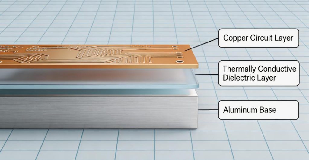
A standard single-layer aluminum PCB consists of three layers:
Copper circuit layer — This is where components are soldered and current flows. Copper thickness typically ranges from 1 oz to 3 oz depending on the current requirements of the design. Heavier copper means better current handling and also better lateral heat spreading from component pads.
Thermally conductive dielectric layer — This is the most critical layer from a thermal standpoint. It sits between the copper circuit layer and the aluminum base. The dielectric layer must provide electrical insulation while allowing heat to pass through as efficiently as possible. These two requirements create a fundamental trade-off: thicker dielectric provides better insulation but increases thermal resistance.
Aluminum base layer — This is the structural and thermal spreading layer. Once heat passes through the dielectric, it enters the aluminum base and spreads laterally before being conducted to the heatsink, chassis, or ambient environment.
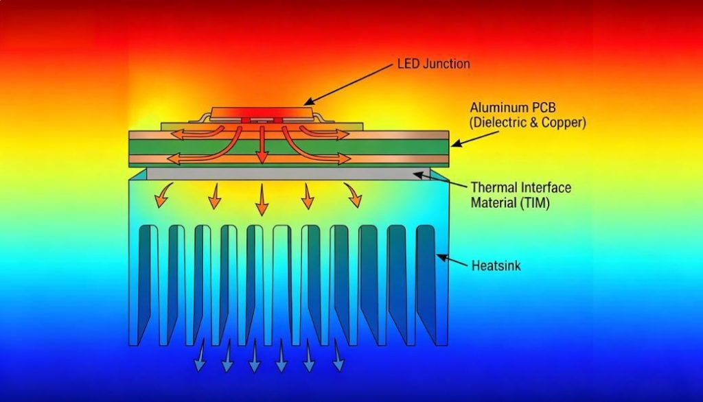
The complete thermal path from a component to the ambient environment looks like this:
Component junction → Solder joint → Copper layer → Dielectric layer → Aluminum base → Thermal interface material → Heatsink or chassis → Ambient
Every layer and interface in this path adds thermal resistance. Reducing total thermal resistance is the goal, and the dielectric layer is usually where the most improvement is possible — and where the most trade-offs need to be managed.
The Dielectric Layer: Where Thermal Performance Is Actually Determined
Many engineers focus on the aluminum base when evaluating aluminum PCBs. In practice, the dielectric layer has a much larger influence on thermal resistance.
The thermal resistance of a flat layer can be expressed as:
Where:
- is thermal resistance in °C/W
- is the thickness of the layer in meters
- is the thermal conductivity of the material in W/m·K
- is the effective heat transfer area in m²
For a typical aluminum PCB dielectric layer, is small — often between 75 µm and 200 µm — but is also much lower than that of the aluminum base. Standard dielectric materials used in aluminum PCBs may have thermal conductivities ranging from around 1 W/m·K on the lower end to 3–4 W/m·K for mid-range materials, and higher for specialty formulations.
Compare this to the aluminum base itself, which conducts heat roughly 50–100 times more efficiently. The dielectric layer is the weak link in the thermal chain, even though it is the thinnest layer.
This means that two aluminum PCBs with the same aluminum thickness and purity can have very different real-world thermal performance if their dielectric materials differ.
When evaluating aluminum PCB materials, it is worth asking:
- What is the dielectric layer thermal conductivity, and how was it tested?
- What is the dielectric thickness?
- What is the dielectric breakdown voltage?
- What is the thermal impedance of the complete board under representative test conditions?
Thermal conductivity alone does not tell the full story. Two dielectric materials with the same rated thermal conductivity but different thicknesses will have different thermal resistance. The combination of and — not alone — determines performance.
Thermal Resistance: A More Useful Metric
Rather than comparing thermal conductivity numbers in isolation, engineers working on thermal-critical designs often find it more useful to calculate or measure the thermal resistance of the dielectric layer directly.
For a 100 µm thick dielectric with a thermal conductivity of 2 W/m·K, applied over a 10 mm × 10 mm component pad:
For a 150 µm thick dielectric with the same thermal conductivity over the same area:
That 50µm difference in thickness adds 0.25°C/W to the thermal path. For a component dissipating 10W, that is an additional 2.5°C of temperature rise across the dielectric layer alone.
These numbers seem small in isolation, but they add up when combined with other resistances in the path, and they become significant in high-power-density designs where thermal budgets are tight.
LED Lighting: Why Thermal Management Matters
High-power LEDs are temperature-sensitive devices. The performance and lifespan of an LED are closely related to the temperature at the p-n junction inside the package, referred to as junction temperature .
As junction temperature increases:
- Luminous flux output decreases — the LED produces less light at higher temperatures, a characteristic called thermal droop
- Forward voltage shifts
- Color temperature and CIE chromaticity coordinates can drift
- Lumen maintenance over time degrades more rapidly
- The probability of early failure increases
LED manufacturers typically specify a maximum junction temperature — commonly in the range of 125°C to 150°C — and provide lumen maintenance curves (L70, L90) that assume the LED operates at a specific test point temperature.
The practical challenge is that the engineer controls the PCB and thermal design, not the junction temperature directly. The relationship between the two is:
Where:
- is junction temperature
- is ambient temperature
- is the power dissipated by the LED
- is the total thermal resistance from junction to ambient
And can be broken down further:
Where:
- is from junction to the bottom of the LED package — specified by the LED manufacturer
- is through the PCB stack — depends on the aluminum PCB design
- is through the thermal interface material between PCB and heatsink
- is from heatsink to ambient — depends on heatsink design and airflow
The aluminum PCB directly affects . A lower thermal resistance PCB gives more headroom in the thermal budget for the other elements in the chain.
In LED street lights, high-bay fixtures, and automotive headlights, the ambient temperature is often already elevated, and the heatsink may be limited in size or airflow. In these conditions, minimizing becomes important.
Power Modules: Different Requirements, Same Principles
In power conversion applications — AC-DC power supplies, DC-DC converters, motor drives, solid-state relays, inverter stages — the thermal challenges are similar in principle but different in detail.
Power components such as MOSFETs, IGBTs, and rectifier diodes dissipate heat primarily as a function of:
- Conduction loss: for MOSFETs
- Switching loss: dependent on switching frequency, voltage, and current waveforms
- Gate drive loss
- Body diode recovery loss
At higher switching frequencies, switching losses increase. At higher load currents, conduction losses dominate. In either case, the heat must go somewhere, and the PCB is often the primary thermal path for surface-mounted components.
Unlike LED applications where the heat source is relatively uniform and the component footprint is the main pad, power modules often have multiple heat sources on the same board with different power densities. The copper layer plays an important role in spreading heat from high-power-density components before it reaches the dielectric.
For this reason, copper thickness matters in power module aluminum PCBs. A heavier copper layer — 2oz or 3oz — can spread heat more effectively across the aluminum base before it needs to pass through the dielectric, which partially compensates for a less conductive dielectric.
In high-voltage power applications, the dielectric layer also needs to meet breakdown voltage requirements. This introduces a real design tension: the thinner the dielectric, the lower the thermal resistance, but the lower the breakdown voltage. For 24V LED driver circuits, a thinner dielectric may be acceptable. For mains-connected power supplies operating at 230V or higher, the dielectric must meet the relevant safety standard requirements, which typically means a thicker layer.
Aluminum PCB Design Considerations
Copper thickness and current capacity
The current-carrying capacity of a copper trace depends on width, thickness, and acceptable temperature rise. For high-power LED or power applications, 2 oz copper is common. 3 oz copper provides more current capacity and better heat spreading but requires tighter attention to etching tolerances.
Component pad design
The thermal pad under a power component should be sized appropriately to maximize heat transfer area through the dielectric. A component with a 5 mm×5 mm exposed pad has a much smaller thermal contact area than one with a 10 mm×10 mm pad. Designers should not reduce pad sizes unnecessarily for routing convenience in thermal-critical applications.
Solder mask over the aluminum base
The backside of an aluminum PCB is usually bare aluminum. If the board is to be mounted to a heatsink using a thermal interface material, the surface condition of the aluminum base — flatness, oxidation, surface roughness — affects thermal contact resistance. This should be considered in the manufacturing and assembly process.
Via usage
Unlike standard FR-4 designs where thermal vias are sometimes used to transfer heat from one copper layer to another, standard aluminum PCBs are typically single-layer or double-layer designs without through-hole plating to the aluminum base. Attempting to use vias to connect copper directly to the aluminum base in a standard process creates a short circuit through the dielectric layer. Some specialized processes allow thermal connections to the metal core, but this requires specific design intent and fabrication support.
Board dimensions and mechanical mounting
Aluminum PCBs are stiffer than FR-4 PCBs of equivalent thickness and have different coefficients of thermal expansion. In applications where the board is mechanically mounted to a housing or heatsink, the mounting method — screw torque, thermal pad compliance, contact area — can significantly affect the thermal resistance between the aluminum base and the heatsink.
What FR-4 Cannot Do in These Applications
It is worth being specific about the limitation of FR-4 in high-power LED and power module applications, because it is sometimes assumed that adding thermal vias to a standard FR-4 board is an adequate substitute.
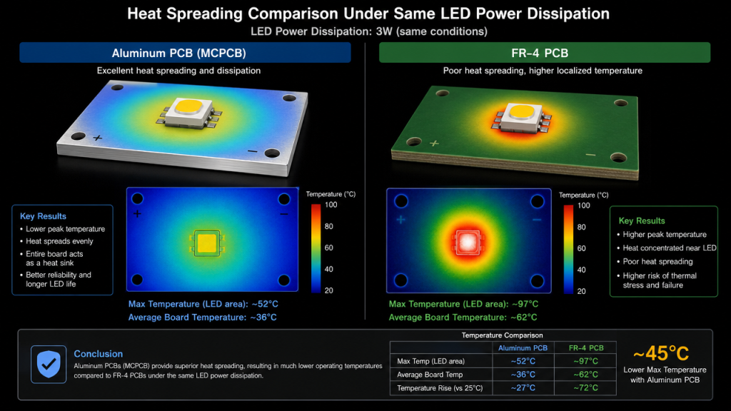
Thermal vias in FR-4 can improve vertical heat transfer, but the thermal conductivity of FR-4 itself remains low. Copper-filled vias improve the local thermal path but do not change the base material limitation. For component power dissipation in the range of a few watts over a small pad area, FR-4 with thermal vias may be acceptable. For higher power densities or applications where junction temperature management is critical to long-term reliability, the aluminum PCB approach provides a fundamentally better thermal path.
The difference is not marginal. The thermal conductivity gap between aluminum and FR-4 is roughly two to three orders of magnitude. Even accounting for the dielectric layer in an aluminum PCB reducing that advantage, the practical thermal resistance of an aluminum PCB board stack is typically significantly lower than an FR-4 equivalent under the same conditions.
Selecting the Right Aluminum PCB Material
Material selection depends on the specific requirements of the application. The main variables to evaluate are:
Thermal conductivity of the dielectric — Higher is better for thermal performance, but cost increases and in some cases processability or reliability trade-offs apply.
Dielectric thickness — Must balance thermal resistance against electrical isolation requirements. Applications with higher working voltages require more isolation.
Operating temperature range — The dielectric material must remain stable across the full operating temperature range of the application, including storage and transportation temperatures.
CTE compatibility — Coefficient of thermal expansion of the dielectric and copper layers affects long-term reliability through thermal cycling. This is relevant in automotive, outdoor lighting, and industrial applications with wide temperature swings.
UL and safety certifications — For end products requiring UL, CE, or other certifications, the PCB material should carry the appropriate approvals.
Closing Thoughts
Aluminum PCBs are not a universal solution for all thermal problems in electronics, but in high-power LED lighting and power module applications, they address a real limitation of FR-4 by providing a direct and efficient thermal path from the component to the board’s metal base.
The effectiveness of an aluminum PCB in practice depends more on the dielectric layer properties and the total assembly thermal path than on the aluminum base alone. Engineers who understand this are better positioned to specify the right material, design the right layout, and avoid the frustration of returning to the thermal problem after the first prototype.
When thermal budgets are tight — in outdoor lighting, automotive electronics, industrial power supplies, or high-density LED modules — getting the PCB thermal design right from the beginning is almost always less expensive than fixing it later.
FAQ
What is the difference between aluminum PCB and FR-4 PCB for thermal performance?
FR-4 laminate has a thermal conductivity of roughly 0.3 W/m·K. The aluminum base layer in a metal core PCB is typically in the range of 150–200 W/m·K. However, the relevant comparison for heat transfer is not the base material alone. The dielectric layer in an aluminum PCB adds thermal resistance that must be accounted for in the total path from component to heatsink. Even so, for high-power LED and power module applications, aluminum PCBs typically offer a significantly lower board-level thermal resistance than FR-4 under equivalent conditions.
Can an aluminum PCB replace a heatsink?
No. An aluminum PCB spreads and conducts heat away from components, but the heat still needs to leave the board. In most high-power applications, the aluminum base is mounted against a heatsink, chassis, or thermally conductive housing using a thermal interface material. The PCB reduces the thermal resistance within the board stack, but the heatsink or cooling structure is still required to manage the total heat load.
Why does the dielectric layer matter more than the aluminum base?
The aluminum base has high thermal conductivity and is not the limiting factor in most designs. The dielectric layer sits between the copper circuit layer and the aluminum base, and it must simultaneously provide electrical isolation and allow heat to pass through. Because its thermal conductivity is much lower than the aluminum — often by a factor of 50 or more depending on material — it is typically the dominant source of thermal resistance in the board stack. Reducing dielectric thickness or increasing its thermal conductivity has a greater effect on overall board thermal resistance than changing the aluminum thickness.
How do I calculate the thermal resistance of an aluminum PCB dielectric layer?
The thermal resistance of a flat, uniform layer is:
Where is the dielectric thickness in meters, is the thermal conductivity in W/m·K, and is the effective heat transfer area in square meters. For a more accurate result, the area should reflect the actual component footprint or thermal pad size rather than the total board area. In practice, the dielectric thermal resistance should be summed with all other resistances in the path — junction to case, thermal interface material, and heatsink to ambient — to estimate total junction temperature at a given power level.
What thermal conductivity should I specify for an aluminum PCB dielectric?
There is no single correct answer. The appropriate dielectric thermal conductivity depends on the component power dissipation, available heatsink and airflow, junction temperature limit, operating voltage, and thermal budget. Higher thermal conductivity dielectrics generally cost more and may have different thickness or breakdown voltage characteristics. A better approach than specifying a thermal conductivity target in isolation is to calculate the maximum allowable dielectric thermal resistance based on your full thermal budget, then identify materials that meet that resistance requirement while also satisfying voltage isolation requirements.
Can I use through-hole vias to improve thermal performance on an aluminum PCB?
In a standard aluminum PCB construction, the copper circuit layer is electrically isolated from the aluminum base by the dielectric layer. A standard plated through-hole via connects copper layers and passes through the dielectric, which means it would create a short circuit between the copper and the aluminum if it contacted the base material. Conventional thermal via strategies used in FR-4 designs do not translate directly to aluminum PCB. Some specialized constructions allow connections to the metal core, but these require specific design consideration and fabrication process support from the manufacturer.
What causes aluminum PCBs to fail in thermal cycling applications?
Thermal cycling creates mechanical stress due to mismatch between the coefficients of thermal expansion of different layers. Copper, dielectric, and aluminum all expand and contract at different rates with temperature change. Over many cycles, this can lead to delamination at the copper-dielectric or dielectric-aluminum interface, solder joint cracking at component pads, or microcracking within the dielectric layer. The severity depends on the temperature range, cycle frequency, dielectric material properties, copper thickness, pad geometry, and assembly quality. Applications with wide and frequent temperature swings — automotive, outdoor lighting, industrial equipment — should consider CTE compatibility alongside thermal conductivity when selecting materials.
Is aluminum PCB suitable for high-voltage power supply designs?
It depends on the dielectric thickness and material, the working voltage, and the applicable safety standards. For low-voltage LED driver circuits, a thinner dielectric with lower breakdown voltage may be sufficient. For mains-connected power supplies or applications requiring compliance with safety standards such as IEC 60950, IEC 62368, or others, the dielectric must provide adequate creepage and clearance distances and meet the breakdown voltage requirements of the relevant standard. Thicker dielectrics provide higher breakdown voltage but also increase thermal resistance. This trade-off must be evaluated for each application.
How does copper thickness affect thermal performance in aluminum PCBs?
Copper thickness affects thermal performance in two ways. First, a thicker copper layer spreads heat laterally from the component pad before it reaches the dielectric layer, which distributes the heat over a larger area and effectively reduces the local thermal resistance. Second, thicker copper improves current-carrying capacity and reduces resistive heating in power traces. For power module applications with high current paths, 2oz or 3oz copper is common. The trade-off is that thicker copper is harder to etch to fine line widths and may require tighter process control during fabrication.
What is the role of thermal interface material between the aluminum PCB and heatsink?
The thermal interface material fills microscopic air gaps between the aluminum PCB backside and the heatsink surface. Air is a poor thermal conductor, and even surfaces that appear flat under visual inspection have surface roughness that traps air at the interface. Thermal interface materials — thermal pads, thermal grease, phase-change materials — displace this air and reduce contact resistance. The performance of the thermal interface material, its thickness under mounting pressure, and the contact area and flatness of the mating surfaces all contribute to the total thermal resistance at this interface. In some designs, this interface contributes as much to total junction temperature as the PCB dielectric itself, which is why it should not be overlooked in the system-level thermal design.



0 Comments