




Drilling is one of the most fundamental processes in PCB manufacturing, and the method you choose directly affects cost, board density, reliability, and manufacturability. Two technologies dominate the field: mechanical drilling, which uses carbide or diamond-coated bits to physically cut through the board, and laser drilling, which uses focused energy to ablate material layer by layer. Each method has distinct capabilities, limitations, and cost structures. Understanding when to use each approach is critical for designers working on anything from industrial control boards to high-density HDI smartphones.
This guide explains how both technologies work, compares their performance across key dimensions, and provides concrete decision criteria based on hole size, board thickness, density requirements, and cost constraints. Whether you are designing a six-layer motor controller or a sixteen-layer RF module, the drilling method you choose will shape what is manufacturable, what is reliable, and what fits your budget.
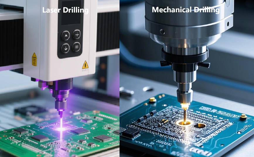
Mechanical Drilling: Process and Capabilities
How Mechanical Drilling Works
Mechanical drilling uses high-speed rotating drill bits, typically made from tungsten carbide with optional diamond coatings for extended life. The bit penetrates the board stack, cutting through copper, resin, and glass fiber to create a cylindrical hole. The process involves several steps: positioning the board under the drill spindle using CNC coordinates, drilling the hole at speeds that can exceed 100,000 RPM, removing burrs from entry and exit points, and performing a desmear process to clean resin residue from the hole wall before plating.
The drill bit is the consumable component. As it cuts, friction and heat wear down the cutting edges. A single bit may drill anywhere from 3,000 to 10,000 holes before it must be replaced, depending on hole size, board material, and spindle parameters. Dull bits produce rough hole walls, increase drilling force, and raise the risk of breakage.
Drill Size Range and Limitations
Mechanical drilling can produce holes from approximately 0.15 mm up to 6.5 mm in diameter. In practice, most PCB vias fall between 0.2 mm and 1.0 mm. Holes smaller than 0.15 mm are difficult to drill reliably because the bit becomes extremely fragile. At that scale, even slight misalignment, material inconsistency, or excessive feed rate can snap the bit.
The maximum achievable aspect ratio—the ratio of hole depth to diameter—is typically 10:1, with some manufacturers pushing to 12:1 under controlled conditions. For a 1.6 mm thick board, this means a 0.15 mm hole is near the practical limit. Thicker boards require proportionally larger holes, or the risk of drill breakage and incomplete plating rises sharply.
Hole Quality Characteristics
Mechanically drilled holes have textured walls. The cutting action of the bit leaves microscopic grooves and occasionally small tears in the resin matrix. Copper foil at the hole edge can be pulled inward, creating burrs. Glass fibers may protrude into the hole or cause localized roughness. After drilling, resin smear—softened resin that has been dragged across the copper surface—must be removed through chemical desmear or plasma treatment to ensure proper plating adhesion.
Drill bit condition directly affects hole quality. A sharp bit produces cleaner walls and less smear. A worn bit generates more heat, increases smear, and can cause positional drift or incomplete penetration. Monitoring bit life and replacing bits on schedule is a key part of process control in mechanical drilling.
Throughput and Cost
Mechanical drilling is a mature, high-throughput process. A modern CNC drilling machine can drill several hundred holes per minute across multiple boards simultaneously, depending on hole size and stack height. Equipment cost is moderate compared to laser systems, and many PCB manufacturers already have extensive mechanical drilling capacity.
The consumable cost is drill bits. For high-volume production with small holes, bit replacement becomes a significant line item. However, for boards with larger holes and moderate complexity, mechanical drilling remains the most cost-effective option by a wide margin. The process scales well, and per-hole cost decreases as volume increases.
Laser Drilling: Process and Capabilities
How Laser Drilling Works
Laser drilling uses focused laser pulses to vaporize material rather than mechanically cutting it. Two types of lasers are commonly used in PCB manufacturing: CO2 lasers and UV lasers. CO2 lasers operate at a wavelength of 10.6 micrometers, which is strongly absorbed by organic resins and dielectric materials. UV lasers operate at 355 nanometers, a wavelength that can ablate copper and glass fiber as well as resin. CO2 lasers are faster and more common for drilling blind vias through dielectric layers. UV lasers provide finer control and are used for conformal drilling or applications requiring higher precision.
The drilling process is pulsed. Each laser pulse removes a thin layer of material, and the depth is controlled by the number of pulses and the energy per pulse. For a microvia, the laser typically needs to penetrate only a single layer of prepreg or core material, often 50 to 100 micrometers thick. The process is non-contact, which eliminates mechanical stress and tool wear.
After laser drilling, a thin carbonized layer, or char, remains on the hole wall. This must be removed through desmear—usually plasma cleaning or light chemical etching—before the hole can be plated. The char forms because organic resin decomposes under intense heat, leaving behind carbon residue.
Via Types Enabled by Laser Drilling
Laser drilling is the enabling technology for microvias and HDI board construction. A microvia is a small-diameter via, typically 50 to 150 micrometers, that connects one layer to an adjacent layer. Unlike through-holes, microvias do not span the entire board. This allows for much higher routing density, shorter signal paths, and better electrical performance in high-speed designs.
Blind vias connect an outer layer to one or more inner layers but do not go all the way through the board. Buried vias connect inner layers without reaching the surface. Both are produced using sequential lamination: the board is built up in stages, and laser drilling is performed after each lamination step to connect the newly added layers.
Stacked microvias are multiple microvias aligned vertically, allowing signals to traverse several layers in a compact footprint. Staggered microvias are offset horizontally, which avoids the need for via filling and provides more routing flexibility. Both approaches are standard in smartphone motherboards, high-end graphics cards, and dense digital modules.
Hole Quality and Precision
Laser-drilled holes are remarkably consistent in diameter, often within ±5 micrometers. The hole wall is smooth because there is no mechanical cutting action to tear or distort the material. However, the thermal process does leave char, and the edge quality depends on laser parameters such as pulse energy, repetition rate, and focus depth. Overdriving the laser can cause excessive carbonization or melting of surrounding resin, while underdriving it results in incomplete material removal.
Because laser drilling is a layer-by-layer process, it does not suffer from the aspect ratio limitations of mechanical drilling. A laser can drill a 0.1 mm microvia through a 0.1 mm dielectric layer with no difficulty, regardless of the total board thickness. The limitation is that each microvia connects only adjacent layers, so deep connections require stacked or staggered via structures.
Throughput and Cost
Laser drilling throughput depends on hole size, material type, and laser power. High-power CO2 lasers can drill tens to hundreds of microvias per second. UV lasers are slower but more precise. For boards with thousands of microvias, the process is still faster than mechanically drilling holes of equivalent size would be—if mechanical drilling could even achieve those sizes.
The capital cost of laser drilling equipment is high. A production-grade CO2 or UV laser system represents a significant investment. However, there are no consumable drill bits to replace, and the laser source itself can last for millions of pulses before requiring maintenance. For low-volume or prototype work, the lack of setup time and tool changes makes laser drilling attractive. For high-volume HDI production, the cost per microvia becomes acceptable because the technology is the only viable option.
Side-by-Side Comparison
| Aspect | Mechanical Drilling | Laser Drilling |
|---|---|---|
| Hole diameter range | 0.15 mm to 6.5 mm | 0.05 mm to 0.15 mm (microvias) |
| Maximum aspect ratio | 10:1 to 12:1 | 1:1 (single-layer blind via) |
| Hole wall quality | Textured, burrs, resin smear | Smooth, no mechanical stress, char |
| Applicable via types | Through-hole, large blind vias | Microvia, blind via, HDI structures |
| Drilling speed | Several hundred holes per minute | Tens to hundreds of holes per second |
| Equipment cost | Moderate | High |
| Consumable cost | Drill bits, frequent replacement | Minimal, laser source long-lived |
| Desmear requirement | Heavy (resin smear) | Moderate (char removal) |
| Typical board types | Standard multilayer, thick boards | HDI, high-density interconnect |
Hole Diameter and Density
Mechanical drilling cannot reliably produce holes below 0.15 mm. Drill bits at that diameter are fragile and prone to breakage, especially in boards with heavy glass fiber content or inconsistent material properties. Laser drilling, by contrast, excels in the microvia range. A 0.1 mm or even 0.08 mm diameter hole is routine for laser systems, and this capability is what makes fine-pitch BGA fanout and dense HDI routing possible.
For holes larger than 0.3 mm, mechanical drilling is faster and more economical. Laser drilling large holes is inefficient because the laser must make many passes to remove enough material, and the thermal load can damage surrounding areas.
Aspect Ratio Limitations
Mechanical drilling is constrained by the rigidity of the drill bit. Drilling a small hole through a thick board creates a high aspect ratio, and the bit can flex, wander, or snap. At 10:1, a 0.2 mm hole can go through a 2.0 mm board, but quality and yield drop as you push that limit. Thicker boards or smaller holes require larger drill diameters to stay within safe aspect ratios.
Laser drilling does not have this limitation because it ablates material layer by layer rather than penetrating the full thickness in one pass. However, laser drilling is fundamentally limited to blind vias. It cannot create through-holes spanning the entire board. For that, mechanical drilling is the only option.
Hole Wall Quality
Mechanically drilled holes have rough walls. The bit’s cutting edges create grooves, and the mechanical stress can cause microcracks in the resin or delamination at layer interfaces. Resin smear is a persistent issue: softened resin is dragged across the copper pad, insulating it from the plating bath unless aggressive desmear chemistry is used. Glass fibers protruding into the hole can also interfere with plating uniformity.
Laser-drilled holes are smooth because no physical tool touches the material. There is no mechanical stress, no smear in the traditional sense, and no risk of tearing the copper foil. The tradeoff is char. The carbonized layer left by the laser must be removed, typically with plasma or permanganate desmear, to ensure the copper plating adheres properly. If char is not fully removed, it can cause plating voids or weak adhesion, leading to reliability failures.
Cost Structure
Mechanical drilling has moderate equipment cost and high consumable cost. Drill bits wear out quickly, especially when drilling small holes or working with hard materials. For a high-volume production run with hundreds of thousands of holes, bit replacement becomes a significant expense. However, the per-hole cost is low, and the process is highly parallelized.
Laser drilling has high equipment cost and low consumable cost. The laser source and optics are expensive, but there are no bits to replace. For prototype or low-volume work, laser drilling avoids setup time and tool changes, making it more efficient. For HDI boards where microvias are required by design, laser drilling is not optional—it is the only way to achieve the necessary hole sizes and layer interconnections.
When to Use Mechanical Drilling
Through-Hole Vias
If your design includes through-hole vias that span the entire board thickness, mechanical drilling is the only practical choice. Laser drilling cannot create through-holes because it ablates material one layer at a time and loses focus as it penetrates deeper into the stack. Any via that must connect the top surface to the bottom surface requires a mechanically drilled hole.
Large Diameter Holes
For holes larger than 0.3 mm, mechanical drilling is faster and more cost-effective. Drilling a 0.5 mm or 0.8 mm hole with a laser would require excessive pulses, generate significant heat, and risk damaging adjacent material. Mechanical bits handle large holes easily, and the per-hole cost is negligible compared to laser processing time.
Thick Boards and High Aspect Ratios
Consider an eight-layer industrial control board, 2.4 mm thick, with 0.3 mm diameter vias. The aspect ratio is 8:1, which is within the capability of mechanical drilling but impossible for laser drilling to achieve as a single through-hole. Mechanical drilling remains the standard for thick boards where vias must span multiple layers in one pass.
Cost-Sensitive Standard Multilayer Boards
For high-volume consumer electronics—LED driver boards, power supply controllers, or simple communication modules—mechanical drilling offers the best cost structure. These boards typically have four to eight layers, hole diameters between 0.25 mm and 0.5 mm, and moderate density. The component pitch is forgiving, and there are no microvias. Mechanical drilling provides reliable, repeatable results at the lowest per-board cost.
Example: Injection Molding Machine Main Controller
The main controller board of a hydraulic injection molding machine manages barrel heaters, screw motor control, hydraulic valve drivers, mold-clamping actuators, and thermocouple inputs. The board uses primarily through-hole terminal blocks for power connections, standard 1206 and 0805 resistors and capacitors, SOIC and TSSOP gate drivers and op-amps, and several TO-252 MOSFETs for heater switching. The smallest pitch on the board is 0.65 mm for a few TSSOP digital isolators. The board has six layers, 1.6 mm thick, and hole diameters range from 0.3 mm to 1.0 mm.
Mechanical drilling is the obvious choice. The component pitch is forgiving, there are no area-array packages that require microvias, and the board is produced in quantities of several thousand per year. Drill bit cost is predictable, and the process is well understood. The board operates in an industrial environment where cost control matters, and mechanical drilling delivers reliable results without introducing unnecessary process complexity.
When to Use Laser Drilling
HDI Boards and Microvia Structures
High-density interconnect boards cannot be built without laser drilling. The defining feature of HDI is the use of microvias to increase routing density and reduce layer count. A sixteen-layer smartphone motherboard may use laser-drilled microvias to fan out signals from a 0.4 mm pitch BGA processor, connect dense memory arrays, and route RF traces on inner layers. Mechanical drilling cannot produce holes small enough or achieve the placement density required.
Blind and Buried Via Designs
Sequential lamination processes rely on laser drilling. The board is built in stages: a core is laminated, laser-drilled, plated, and then another layer is added. Blind vias connect the new outer layer to the core, and the process repeats. This allows designers to pack more routing into fewer total layers, reducing board thickness and improving signal integrity. Mechanical drilling cannot create these layer-specific connections because it always goes through the full stack.
High-Density Interconnect and Fine Routing
Consider the CPU carrier board for a high-performance server. The board has over twenty layers, microvias with diameters as small as 0.08 mm, and extremely tight routing pitch to handle thousands of processor I/O signals. Laser drilling is not just preferred in this application—it is the only technology capable of producing the required via sizes and densities. The cost is secondary to functionality.
Example: Six-Axis Industrial Robot Servo Control Board
The servo control board of a six-axis industrial robot processes encoder feedback and generates real-time control signals for the motor drives of the robot’s six joints. The board is built around a 0.8 mm pitch BGA motion controller with over 400 balls, multiple 0.5 mm pitch QFN gate drivers and current-sense amplifiers, and 01005 decoupling capacitors placed densely around the BGA. The board uses a ten-layer HDI stackup with microvias to fan out the BGA signals. The tightest via diameter is 0.1 mm, and several layers are connected through stacked microvias.
Laser drilling is mandatory. The BGA cannot be fanned out with 0.3 mm mechanically drilled vias—the pad pitch is too tight, and the via size would consume too much routing space. The QFN gate drivers have exposed thermal pads that require blind vias for thermal management, and those vias must be small to fit within the pad footprint. Mechanical drilling would make this design impossible to manufacture. Laser drilling provides the precision, density, and layer-specific connections the design requires, and the higher cost is justified by the complexity and performance demands of the application.
Rapid Prototyping and Low-Volume Production
Laser drilling does not require tool changes or bit inventory management. For prototype boards or small production runs, this reduces setup time and avoids the risk of drill breakage. A contract manufacturer can laser-drill a batch of HDI prototypes without the lead time and cost overhead of setting up mechanical drilling programs, managing bit wear, and dealing with breakage-related yield loss.
Design Considerations and Rules
Mechanical Drilling Design Rules
The most critical rule for mechanical drilling is aspect ratio. Keep the ratio of hole depth to diameter below 10:1 to ensure reliable drilling and plating. For a 1.6 mm board, this means hole diameters should not go below 0.16 mm. For 2.0 mm boards, stay above 0.2 mm.
Hole-to-hole spacing should be at least two times the hole diameter to prevent drill wander and ensure structural integrity. Hole-to-copper clearance—the distance from the edge of the drilled hole to adjacent copper features—should be at least 0.2 mm to avoid nicking traces or planes during drilling.
Drill breakage risk increases with small holes, thick boards, and materials with heavy glass fiber content. If your design pushes aspect ratio limits, consult with your manufacturer early to confirm capability and adjust hole sizes if needed.
Laser Drilling Design Rules
Microvia diameter typically ranges from 0.05 mm to 0.15 mm, with 0.1 mm being common for HDI designs. The depth of a laser-drilled microvia is limited to a single dielectric layer, usually 50 to 100 micrometers. If you need to connect non-adjacent layers, you must use stacked or staggered microvias.
Stacked microvias require filled plating. Each via must be copper-filled and planarized before the next layer is added, or voids will form that trap air or flux and create reliability problems. Staggered microvias avoid the filling requirement by offsetting each via horizontally, but they consume more board real estate.
When designing microvia fanout for fine-pitch BGAs, calculate the required via density early. A 0.4 mm pitch BGA may require two or three rows of microvias around the package to escape all signals. Ensure your stackup and via placement support the routing you need without violating minimum spacing rules.
Hybrid Drilling Strategies
Most HDI boards use a combination of mechanical and laser drilling. Laser drilling creates microvias in high-density areas—under BGAs, between tightly routed signal layers, or for blind vias in sequential lamination. Mechanical drilling creates through-holes for connectors, mounting holes, and larger vias in less dense regions.
This hybrid approach optimizes cost. You pay for laser drilling only where it is necessary, and use mechanical drilling everywhere else. When planning your stackup, identify which vias must be microvias and which can be mechanically drilled, and work with your manufacturer to define the most cost-effective drilling strategy.
Quality Control and Failure Modes
Mechanical Drilling Common Issues
Drill breakage is the most visible failure mode. Causes include excessive feed rate, dull bits, misalignment, or attempting to drill holes with aspect ratios beyond equipment capability. Broken bits can damage boards and require rework or scrapping.
Positional drift occurs when a worn bit flexes during drilling, causing the hole to be offset from its intended location. This can result in open circuits or shorts if the hole misses the pad or intersects adjacent copper.
Hole wall roughness and copper burrs result from dull bits or improper drilling parameters. Rough walls increase plating difficulty and can trap contaminants. Burrs must be removed through deburring processes, or they can cause shorts or interfere with component assembly.
Laser Drilling Common Issues
Char residue is the primary concern. If the carbonized layer is not fully removed during desmear, the copper plating will not adhere properly. This can cause weak joints, plating voids, or complete adhesion failure. The desmear process must be carefully controlled, and cross-sectional analysis is often used to verify char removal.
Hole diameter inconsistency can result from unstable laser power, focus drift, or material variation. Laser systems require regular calibration and maintenance to ensure pulse energy and focus depth remain within specification.
Resin melting and redeposition can occur if the laser energy is too high. Molten resin can flow back into the hole or onto adjacent surfaces, creating defects that interfere with plating. Proper parameter tuning and material selection minimize this risk.
Inspection and Control
Optical inspection systems measure hole diameter, position, and count. Automated optical inspection catches missing holes, oversized holes, and positional errors before the board moves to plating.
Cross-sectional analysis is the gold standard for evaluating hole wall quality. A sample board is cut, polished, and examined under a microscope to assess copper thickness, plating uniformity, char removal, and the presence of voids or cracks. This destructive test provides the most detailed view of drilling and plating quality.
Electrical testing verifies that all vias are conductive and that there are no shorts between adjacent features. Continuity testing catches open vias, and isolation testing detects shorts caused by drill wander, burrs, or plating defects.
Conclusion
Mechanical drilling and laser drilling are not competing technologies—they are complementary. Mechanical drilling is the workhorse for through-holes, large vias, and cost-sensitive standard boards. Laser drilling is the enabler for microvias, HDI structures, and high-density interconnect designs that would be impossible to manufacture otherwise.
Choose mechanical drilling when your design includes through-hole vias, hole diameters above 0.3 mm, or when minimizing cost is the priority. Choose laser drilling when your design requires microvias below 0.15 mm, blind vias for HDI stackups, or fine-pitch BGA fanout. For mixed requirements, use a hybrid approach: laser drill where density demands it, and mechanically drill everywhere else.
Drilling technology is a fundamental manufacturing constraint that shapes what you can design. Understanding the capabilities and limitations of both methods allows you to make informed decisions early in the design process, avoid costly redesigns, and ensure your boards are manufacturable, reliable, and cost-effective.
If you are evaluating drilling methods for an upcoming design or need guidance on HDI stackup planning, download our PCB Manufacturability Design Guide for detailed design rules, capability tables, and decision flowcharts.
FAQ
What is the smallest hole size mechanical drilling can achieve?
Mechanical drilling can reliably drill holes down to 0.15 mm in diameter, though0.20 mm is more common in production due to drill bit fragility below that size. Holes smaller than 0.15 mm require laser drilling.
Can laser drilling create through-hole vias?
No. Laser drilling is limited to blind vias and microvias within a single dielectric layer. Through-hole vias spanning the entire board thickness require mechanical drilling.
What is the maximum aspect ratio for mechanically drilled holes?
The practical limit is 10:1 to 12:1. For a 1.6 mm thick board, the minimum mechanically drilled hole diameter is approximately 0.15 mm. Higher aspect ratios increase drill breakage risk and copper plating difficulty.
Why does laser drilling produce char on the hole wall?
CO2 lasers vaporize resin through thermal ablation, which carbonizes organic material at the hole wall. This char layer must be removed through plasma cleaning or chemical desmear before copper plating to ensure proper adhesion.
Is laser drilling more expensive than mechanical drilling?
It depends on volume and hole size. Laser drilling equipment is more expensive, but has no consumable costs. For high-volume standard boards with larger holes, mechanical drilling is cheaper per hole. For HDI boards with thousands of microvias or low-volume prototypes, laser drilling is often more cost-effective overall.
Can I mix mechanical and laser drilling on the same board?
Yes. This is standard practice in HDI designs. Laser drilling creates microvias in high-density areas such as under BGA packages, while mechanical drilling creates through-holes and larger vias elsewhere on the same board.
What causes drill bit breakage in mechanical drilling?
Common causes include excessive feed rate, dull bits, high aspect ratios in thick boards, inconsistent laminate hardness, inadequate chip evacuation, and misalignment between the spindle and board stack.
Do stacked microvias require special design considerations?
Yes. Stacked microvias require each via to be copper-filled and surface-planarized before the next layer is laminated. Without filling, voids form in the via stack that can trap gas or flux, leading to reliability failures during thermal cycling.
What is the difference between CO2 and UV laser drilling?
CO2 lasers at 10.6 μm wavelength are absorbed by resin and used to drill through dielectric layers efficiently. UV lasers at 355 nm can ablate copper, glass fiber, and resin, enabling conformal via drilling and better edge quality on thin copper layers. UV lasers offer higher precision but lower throughput.
How do I choose between mechanical and laser drilling for my design?
Use mechanical drilling if your design has through-holes, hole diameters above 0.25 mm, and no fine-pitch BGA fanout requirements. Use laser drilling if your design requires microvias below 0.15 mm, HDI buildup layers, or via-in-pad structures for fine-pitch components. For designs with both requirements, use a hybrid approach.



0 Comments