




Electrostatic discharge is one of the most underestimated threats in PCB manufacturing and repair. A technician walks across a carpeted floor, reaches for a circuit board, and unknowingly delivers thousands of volts through a fingertip. The board passes testing. It ships to the customer. Three months later, it fails in the field. This is not a rare event—industry estimates suggest that 8 to 33 percent of all field failures in electronics have an ESD-related root cause, and the majority of ESD damage is latent, not immediate.
ESD protection is not about preventing dramatic component explosions. It is about preventing invisible degradation that shortens product life, causes intermittent failures, and drives up warranty costs. This guide covers the mechanisms of ESD damage, practical protection strategies for different operational contexts, standard procedures for PCB handling, and methods for identifying whether a failure was ESD-related. Whether you manage a high-volume production line or a small repair bench, the principles and procedures here will reduce losses and improve reliability.
What Is ESD and Why It Matters in PCB Operations
Electrostatic discharge occurs when accumulated charge transfers rapidly between two objects at different electrical potentials. The charge buildup happens through triboelectric effects—friction between dissimilar materials—or through electrostatic induction in the presence of a charged object. Walking across a synthetic carpet, peeling tape off a roll, or sliding a PCB out of a plastic bag can generate thousands of volts.
Two Types of ESD Damage
ESD damage falls into two categories, and the distinction matters for how you design protection and interpret failures.
Catastrophic failure is immediate and obvious. The component stops working entirely. A MOSFET gate oxide ruptures, creating a permanent short. An IC input stage burns through, leaving visible damage under a microscope. These failures are detected quickly, often during in-circuit testing or first power-up.
Latent damage is far more insidious. The ESD event weakens the component but does not destroy it outright. A gate oxide develops microcracks. Junction doping profiles shift slightly. Metallization suffers partial melting that does not immediately open the circuit. The component passes testing because it still functions within specification, but the damage accelerates aging. Under thermal stress, voltage transients, or normal operational cycling, the weakened structure fails weeks or months later. Studies suggest that 90percent of ESD damage is latent, not catastrophic.
This delayed failure mode is why ESD protection cannot be treated as optional. A board that works on your test bench today may fail at the customer site next quarter, and the root cause will be invisible without destructive analysis.
Why PCB Operations Are High-Risk
Printed circuit boards are particularly vulnerable during manufacturing, testing, and repair because they exist in an unprotected state. In the final product, power supply filtering, input protection diodes, and grounded enclosures provide some ESD immunity. But during assembly and rework, the board is exposed. Bare copper traces, unconnected pins, and sensitive analog nodes have no defense against a discharge event.
Human handling is the most common ESD source, but it is not the only one. Automated equipment can generate charge through friction and rapid motion. Non-conductive tooling and fixtures accumulate charge. Even packaging materials—foam inserts, plastic trays, non-shielding bags—can induce charge on a board through field effects or direct contact.
Common ESD Sources in PCB Handling
Understanding where ESD comes from allows you to target protection efforts effectively. The following are the primary charge sources in typical PCB operations.
Human Body Charging
A person wearing synthetic clothing and walking across a vinyl floor can accumulate 10,000 to 30,000 volts of static charge, depending on humidity. Sitting down in a plastic chair or standing up from one generates charge. Reaching into a bin lined with foam does the same. When that charged person touches a grounded object or a PCB, the accumulated charge discharges instantly.
The human body model (HBM) is the industry-standard test for component ESD sensitivity. It simulates a100-picofarad capacitor charged to a test voltage and discharged through a 1,500-ohm resistor—the equivalent of a person touching a pin. Modern CMOS devices often have HBM ratings between 250V and 2,000V. A casual touch from a person charged to 5,000V exceeds those limits.
Tools and Equipment
Soldering irons, if not properly grounded, can accumulate charge at the tip. A floating tip approaching a component can induce charge or directly discharge. The same applies to tweezers, screwdrivers, cutters, and test probes. Even if the tool itself is conductive, if the handle is not grounded and the operator is charged, the tool becomes a discharge path.
Automated equipment poses similar risks. Pick-and-place nozzles, conveyor belts, and vacuum chucks can all generate or transfer charge if not designed with ESD control in mind. A high-speed belt moving across plastic rollers creates friction and charge separation.
Packaging and Transport
Standard plastic bags generate charge when rubbed or separated from their contents. Foam padding—particularly the non-conductive type—is a notorious charge generator. A board placed on regular foam or carried in a standard plastic tray is exposed to charge accumulation and field-induced effects.
The distinction between anti-static, static-dissipative, and static-shielding materials matters. Anti-static materials (often pink or blue) prevent triboelectric charging but do not block external fields. Static-shielding bags (metalized, typically silver) provide a Faraday cage effect, protecting the board from external charges. For transport and storage, shielding bags are the correct choice. For short-term handling within a controlled ESD-protected area, dissipative trays and mats are sufficient.
Environmental Factors
Low humidity accelerates ESD problems. In dry environments—below 30 percent relative humidity—charge dissipates slowly, and accumulated voltages rise. A person in a climate-controlled office at 20 percent RH can easily generate 15,000 to 25,000 volts through ordinary movement. The same actions in a humid environment at 60 percent RH produce far less charge because moisture in the air provides a conductive path for dissipation.
This is why many ESD standards specify humidity targets between 40 and 60 percent. It is not about comfort; it is about charge dissipation rates.
Comprehensive ESD Protection Strategy
Effective ESD control is a system, not a single piece of equipment. The goal is to prevent charge generation where possible, provide controlled dissipation where charge cannot be avoided, and ensure that all conductive objects in the work area share the same electrical potential—ideally earth ground.
Tiered Protection Approach
Not all products require the same level of protection. A microcontroller-based industrial sensor with 2,000V HBM-rated components can tolerate more exposure than a high-speed RF transceiver with 100V components. Tailor your protection level to the sensitivity of what you are handling and the volume of production.
Level 1: Minimum Essential (cost: 500–1,000)
Suitable for low-volume repair or rework of moderately sensitive boards (HBM >1,000V). Includes wrist straps, ESD mats, and astrap tester. Sufficient for occasional handling of industrial control boards, LED drivers, or power supplies with robust components.
Level 2: Standard Production (cost: 2,000–5,000 per workstation)
Appropriate for medium to high-volume assembly of consumer electronics, automotive modules, or computing hardware. Adds ionizers for tool-intensive operations, humidity monitoring, and possibly overhead ESD monitors. Includes proper packaging materials and grounded storage.
Level 3: High-Sensitivity Environment (cost: $10,000+ for facility-wide implementation)
Required for RF modules, high-speed digital boards with sub-100V components, or any application where latent damage is unacceptable (medical, aerospace). Includes continuous monitoring systems, full facility grounding networks, air ionization, and real-time compliance logging.
Personnel Grounding
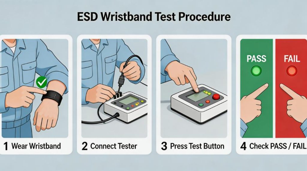
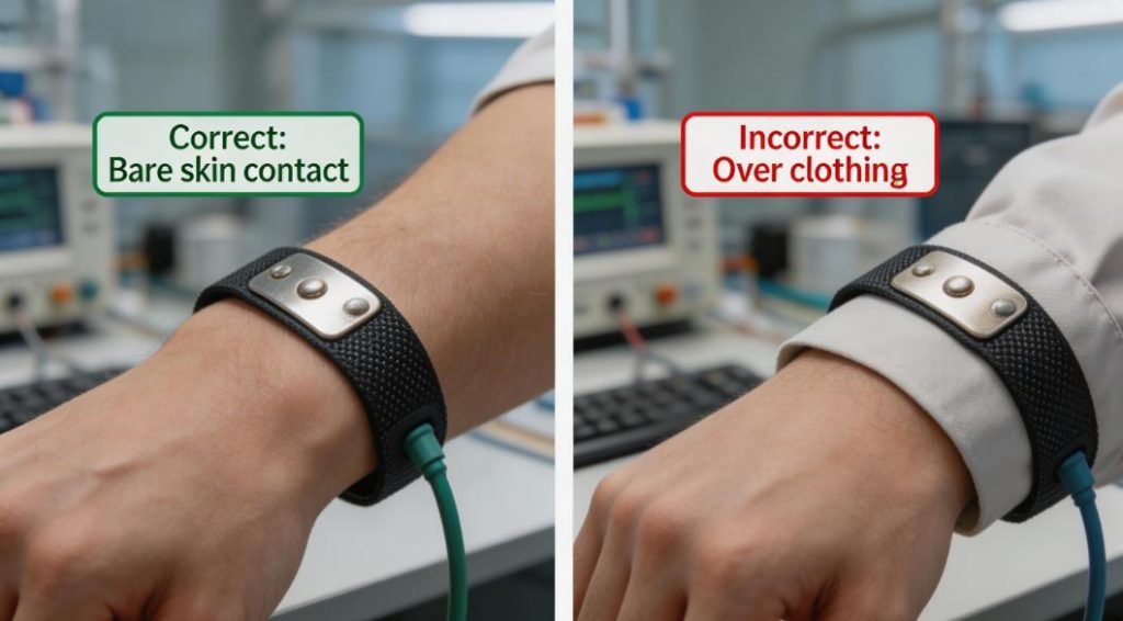
The most fundamental protection is grounding the operator. A wrist strap connects the technician to the workstation ground through a 1-megohm resistor. The resistor is a safety feature—it limits current flow in case the operator accidentally contacts a live voltage, preventing shock. The strap must make contact with bare skin, not be worn over clothing, and must be tested daily.
Wrist strap testers cost 50 to 200 and provide a go/no-go indication ofstrap continuity and resistance. A failed test means either the strap is damaged, the ground connection is broken, or the skin contact is poor. Do not proceed without a passing test.
For mobile operations where wrist straps are impractical—such as walking between multiple stations—heel straps or ESD footwear combined with conductive flooring provide continuous grounding while allowing movement.
Workstation Protection
The ESD mat is the foundation of a protected workstation. It provides a conductive work surface that dissipates charge and establishes a common ground reference. Mats are typically dual-layer: a static-dissipative top surface ( to ohms per square) and a conductive bottom layer. The mat connects to facility ground through a separate wire, not through the wrist strap circuit.
Grounding resistance must be low—less than 1 ohm from the mat to earth ground. Measure this with a ground resistance tester, not a standard multimeter. High resistance indicates a poor ground connection, which defeats the entire protection scheme.
Ionizers neutralize airborne charge and are particularly useful in automated environments where wrist straps are not practical. An ionizer generates both positive and negative ions, which attach to charged particles in the air and neutralize them. This prevents charge accumulation on non-conductive surfaces such as plastic fixtures or product enclosures. Ionizers require maintenance—emitter needles must be cleaned regularly, and ion balance should be checked to ensure equal positive and negative ion output.
Tools and Equipment Grounding
Soldering irons, hot air rework stations, and any handheld tool that contacts the PCB must be grounded. For soldering irons, the tip should be grounded through a 1-megohm resistor to the workstation ground, similar to a wrist strap. This prevents tip-to-board discharge.
Test equipment—oscilloscopes, power supplies, DMMs—should have grounded cases, and probe grounds should be connected before signal probes to avoid discharge through the signal input.
Packaging and Storage
Boards awaiting assembly, in-process, or awaiting shipment must be stored in static-shielding bags or conductive containers. Standard plastic bins and foam are not acceptable. Conductive bins are typically black with carbon-loaded plastic. Shielding bags are metalized and provide a closed Faraday cage when sealed.
Label storage areas and bins clearly. Mix-ups between ESD-safe and non-safe containers are a common source of unintended exposure.
Standard Operating Procedures for PCB Handling
Unpacking and Placement
When removing a board from a shielding bag, do so at an ESD-protected workstation with a grounded mat. Open the bag on the mat, not at a random desk or shipping area. Touch only the board edges, never contact component leads, solder joints, or bare copper. Place the board on conductive foam or directly on the ESD mat.
Before handling any board, put on a wrist strap and test it. This takes five seconds and eliminates the most common failure mode: assuming the strap is working when it is not.
Rework and Repair Operations
Solder rework is a high-risk operation because it involves both ESD exposure and thermal stress. Ensure the soldering iron is grounded and verify ground continuity before turning it on. During heating, the iron tip can accumulate charge if not properly grounded.
When removing or installing components, use one hand whenever possible. If both hands must contact the board, ensure both are grounded. Avoid touching unrelated components or traces while soldering.
After rework, allow the board to cool before moving it. Rapid temperature changes combined with residual charge can induce stress in already-weakened junctions.
Testing Procedures
Test equipment must be grounded before connecting to the board. Connect ground leads first, signal probes second. When disconnecting, reverse the order. Floating test equipment can discharge into the board through signal inputs, particularly on high-impedance analog circuits.
If testing requires the board to be powered, ensure the power supply is grounded and stable before applying voltage. Power-up transients in an ungrounded system can induce ESD-like stress.
Common Mistakes to Avoid
- Wearing a wrist strap but not plugging it in. This happens more often than it should. The strap provides no protection unless connected to ground.
- Using regular plastic bags for storage. They look harmless but generate charge when handled.
- Operating on a non-ESD surface. A standard office desk, even if metal, is not sufficient unless it is part of a grounded ESD system.
- Wearing synthetic clothing in ESD-sensitive areas. Cotton or ESD garments reduce charge generation.
Identifying and Diagnosing ESD Damage
Determining whether a failure was caused by ESD is often difficult without destructive analysis, but certain failure patterns and test results provide strong indicators.
Catastrophic Failure Indicators
If a component fails completely and suddenly—especially an input or I/O pin—ESD is a likely cause. Visual inspection under a microscope may reveal burn marks, melted metallization, or crater formation at bond pads. These are diagnostic of high-energy discharge events.
Electrical testing shows a short or open where the device should be functional. In MOSFETs, gate-to-source or gate-to-drain shorts are classic ESD signatures. In ICs, input protection diodes may be shorted, pulling the pin to either supply rail.
Latent Damage Indicators
Latent damage is harder to catch. The component works but exhibits parameter drift. For example:
- Increased leakage current (measured with a sensitive picoammeter)
- Threshold voltage shifts in analog circuits
- Increased noise or reduced gain in amplifiers
- Intermittent glitches under temperature cycling
Thermal imaging can help. A component with ESD-induced junction damage may run hotter than expected because internal resistance has increased.
Accelerated stress testing—applying voltage, temperature, and humidity stress beyond normal operating conditions—can force latent damage to manifest. This is how reliability labs identify weak populations.
Diagnostic Example: Field Failure Analysis
A batch of industrial motor controllers began failing in the field four to six months after installation. Symptom: intermittent loss of PWM output. Returned boards passed functional testing initially but failed after extended thermal cycling in the lab.
Failure analysis revealed partial gate oxide damage in the PWM driver MOSFETs. The damage pattern was consistent with ESD stress, not electrical overstress from the application. Investigation traced the issue to a repair operation where a contract rework facility had replaced a component on each board without using grounded soldering equipment. The boards worked fine after repair and through final testing, but the latent damage manifested months later under field conditions.
The lesson: lat ent ESD damage can pass all standard quality checks and only fail under long-term operational stress. Prevention is the only reliable defense.
Cost-Benefit Analysis of ESD Protection
The True Cost of ESD Damage
ESD-related losses are rarely limited to the cost of the damaged component. The full cost includes:
- Scrap and rework: 50 to 200 per board depending on complexity
- Test time: Additional cycles to diagnose intermittent issues
- Field failures: Warranty returns, shipping, customer dissatisfaction
- Production delays: Holding shipments while investigating quality escapes
For a mid-volume operation producing 5,000 boards per month at 80 perboard, a 2 percent scrap rate due to ESD represents 8,000 in monthly losses. Over a year, that is nearly $100,000.
Investment in Protection
A functional ESD-protected workstation for a single operator costs 2,000to3,000 including:
- Wrist straps and tester: $100
- ESD mat and grounding hardware: 200–400
- Ionizer (if needed): 500–1,000
- Grounded tools and fixtures: $500
- Shielding bags and conductive storage: $300
- Humidity monitoring: 100–200
If this investment reduces scrap from2 percent to 0.5 percent, the monthly savings is $6,000. The payback period is under six months. For higher-value products such as server motherboards or RF modules, payback can be under one month.
Scaling Protection Across a Facility
Facility-wide ESD control requires additional investment in flooring, building ground networks, and training. For a 20-station assembly line, expect 40,000 to 60,000 in total ESD infrastructure. This scales with product value and volume, and the ROI calculation becomes even more favorable as production increases.
ESD Standards and Compliance
The two primary standards for ESD control are ANSI/ESD S20.20 (North America) and IEC 61340-5-1 (international). Both define requirements for ESD control programs, including personnel grounding, workstation requirements, packaging, and audit procedures.
Certification to these standards requires annual audits and documented procedures for equipment testing, training, and corrective actions. Many OEMs require their contract manufacturers to be ESD-certified as a condition of doing business.
Key compliance elements include:
- Daily wrist strap testing with logged results
- Periodic verification of mat and floor resistance
- Ionizer balance checks
- Training records for all personnel
- ESD control plan documentation
Compliance is not bureaucracy for its own sake. It ensures that protection measures remain effective over time and that problems are caught before they cause field failures.
Conclusion
ESD protection in PCB handling and maintenance is not optional, and it is not only about preventing immediate component failures. The majority of ESD damage is latent—invisible at the time of occurrence but fatal to product reliability months later. A robust ESD control program prevents both types of damage through systematic grounding, controlled environments, proper tooling, and disciplined procedures.
The cost of implementing ESD protection is modest compared to the losses from uncontrolled ESD exposure. A basic workstation setup pays for itself within months through reduced scrap and rework. For high-value or high-volume products, the case is even stronger.
Start with an assessment of your current practices. Test your wrist straps daily. Verify mat grounding. Audit your packaging materials. Train your team on the invisible threat of latent damage. These steps do not require large capital investment, but they require discipline and attention to detail. The long-term reliability of your products depends on it.
If you are building an ESD control program from scratch or need to audit an existing one, download our ESD Protection Checklist for a step-by-step guide to equipment, procedures, and compliance requirements.



0 Comments