




Start With the Right Mental Model: A Schematic Is Not a PCB Layout
To read a circuit diagram schematic, treat it as a map of electrical relationships, not a picture of where parts sit on a board. Symbols represent components or functions. Lines and labels show which pins share an electrical connection. The drawing is arranged to make the circuit’s logic easier to follow, so two symbols placed next to each other may be far apart on the finished PCB.
That distinction solves the first major beginner problem. A schematic, a wiring diagram, and a PCB layout answer different questions:
| Document | Main question it answers | What position means |
| Circuit schematic | What is electrically connected, and how should the circuit work? | Usually arranged for logical clarity |
| Wiring diagram | Which physical wire or terminal connects to which point? | Often related to real installation or harness routing |
| PCB layout | Where are components, pads, copper traces, vias, and board features located? | Represents the physical board |
Reading symbols is only the first level of skill. The second level is being able to follow the connections. The third is understanding why the connected parts produce a particular function. You can copy a circuit onto a breadboard without fully understanding it; you understand it only when you can explain each functional block, predict important voltages or states, and identify what evidence would prove your explanation correct.
Learn Only the Symbols You Need to Begin
You do not need to memorize every schematic symbol before reading your first diagram. Learn the small group that appears in most electronic circuits, then use the reference designator, value, part number, and datasheet to identify anything unfamiliar.
| Marking or symbol | Plain-language meaning | What to check while reading |
| R | Resistor | Resistance value and what current, bias, pull-up, or filtering job it performs |
| C | Capacitor | Capacitance, polarity when applicable, and whether it filters, stores, couples, or times |
| D / LED | Diode or light-emitting diode | Anode/cathode orientation and current path |
| Q | Transistor or MOSFET | Device type, pin names, switching/bias conditions, and datasheet |
| U / IC | Integrated circuit | Exact part number, pin functions, supply pins, and datasheet |
| J / P / CN | Connector | Pin numbers, cable or external interface, and signal direction |
| SW | Switch | Normal drawn state and what changes when actuated |
| VCC, VDD, +5V, +3V3 | Power net | Voltage domain and source |
| GND, AGND, DGND, chassis symbols | Reference or return net | Which ground domain it represents; do not assume every ground is protective earth |
The drawing style may vary. For example, a resistor may be a zigzag or a rectangle. The right response to an unfamiliar symbol is not to guess from its shape. Read the nearby reference and value, check the legend if one exists, and look up the exact component or IC datasheet. PCBTRY’s circuit symbol reference is useful as a lookup page, but the rest of this guide explains how to turn symbols into circuit understanding.
Read Wires, Junctions, and Net Labels as Electrical Connections
Lines on a schematic represent nets: groups of pins that are intended to be electrically connected. A continuous line is the easiest case, but real schematics also use junction dots, power symbols, net labels, ports, and sheet connections to avoid drawing long lines across the page.
Use these rules as your first pass:
- A line ending on a component pin normally connects to that pin.
- A filled junction dot normally means intersecting wires are connected.
- Crossing lines without a dot normally mean no connection, although old drawings or a project-specific legend may use another convention.
- Matching net labels can connect points even when no continuous line is visible.
- Power symbols such as
+5VorGNDcommonly connect every point assigned to that power net. - Label scope matters. A local label may connect only within one sheet, while a global or hierarchical label may connect across sheets.
The last rule prevents a common mistake: treating label text as a comment. In an electronic design tool, a net label often changes connectivity. KiCad, for example, distinguishes local, global, and hierarchical labels, and it assigns a name to every net. When reading source files, use the tool’s net-highlight or search function instead of relying only on your eyes. When reading a PDF, circle each occurrence of the same label and check the title block or drawing notes for its scope.
Find Power, Ground, Inputs, and Outputs Before Following Signals
Begin with the circuit’s boundaries. Find where energy enters, which voltage rails are created, what is used as the reference or return, where information enters, and where the result leaves. This gives every later trace a direction and a purpose.
Ask these questions in order:
- Where does power enter: battery, USB, DC jack, connector, or another board?
- Is there protection before the main rail: fuse, reverse-polarity device, TVS diode, or current limiter?
- Which regulators or converters create rails such as
5V,3V3, or1V8? - Which ground or return domains are shown?
- Which connectors, sensors, switches, antennas, or communication ports are inputs?
- Which LEDs, motors, relays, displays, speakers, loads, or connectors are outputs?
Schematics often place inputs on the left, outputs on the right, positive rails toward the top, and ground toward the bottom. Treat that as a reading aid, not a law. Feedback paths may run from right to left, and crowded or inherited drawings may ignore the convention entirely.
Do not say “ground is where current disappears.” Ground is a chosen reference node and often part of the return path. GND, AGND, DGND, chassis ground, and protective earth can have different meanings. The schematic notes and connection strategy decide whether and where those domains meet.
Break a Large Schematic Into Functional Blocks
A large schematic becomes manageable when you stop reading it one wire at a time. Divide it into functional blocks, then describe the relationship between blocks before studying the components inside each block.
Common blocks include:
- power input and protection;
- voltage regulation;
- sensor or analog front end;
- microcontroller, processor, or logic;
- clock and reset;
- communication interface;
- driver stage;
- output load;
- programming and test access.
For each block, write one sentence:
This block receives ___, changes or controls ___, and sends ___ to ___.
For example: The regulator block receives 9 V from J1, produces the 3.3 V rail, and powers U1 and the sensor connector.
That sentence is more useful than naming every resistor. It gives you a hypothesis that you can test against net labels, pin names, values, and datasheets. If a schematic is hierarchical, the root sheet often acts as a block diagram: inspect it first, then open the child sheet that contains the function you need.
Trace One Signal Path Without Getting Lost
Follow one path only after you have defined its source, destination, reference, and expected state. “Follow the signal” is incomplete advice because a branch, feedback path, or mislabeled assumption can send you in the wrong direction.
Use this small worksheet:
| Field | Question |
| Source | Which pin, connector, sensor, regulator, or block creates the signal? |
| Destination | Which pin, load, or block receives it? |
| Reference | Relative to which ground, differential partner, or reference node is it interpreted? |
| Expected state | Should it be DC, pulsed, analog, digital, active-high, active-low, or conditional? |
| Changes along the path | Which resistor, capacitor, diode, transistor, connector, or IC can alter it? |
| Verification | Which datasheet, test point, simulation, or safe measurement would confirm the interpretation? |
Suppose a pushbutton controls a microcontroller input. Start at the connector or switch, identify the net name, follow it to the IC pin, and note any pull-up resistor or filter capacitor. Then use the IC datasheet to check whether the pin is active-high or active-low. A line alone tells you where the signal goes; the surrounding components and datasheet tell you what state the receiver sees.
For repair work, do not start probing a powered board simply because you found a path. First identify the voltage domain and hazards. High-voltage, mains-connected, or high-energy circuits require suitable training, isolation, instruments, probes, and procedures.
Read Reference Designators, Values, and IC Pins Together
A symbol tells you the component category, but the text around it tells you which physical part and electrical role you are reading. Treat the symbol, reference designator, value, pin number, pin name, and datasheet as one information set.
R7 10 kΩ means resistor number 7 with a nominal value of 10 kΩ. U2 identifies one integrated circuit, but its value or part-number field tells you which device it is. If the symbol says pin 6 is OUT, verify that function in the correct datasheet and package.
IC symbols are frequently arranged by function rather than physical pin order. Inputs may be drawn on the left, outputs on the right, and power pins at the top or bottom even when the package pins are located elsewhere. Some devices are split into units such as U3A, U3B, and U3C; another unit may contain the power pins. Hidden power pins also exist in some libraries and older projects.
Before claiming you understand an IC connection:
- identify the exact manufacturer part number and package;
- match the symbol pin number to the datasheet pinout;
- find every unit of the same reference designator;
- locate supply, ground, enable, reset, clock, and exposed-pad connections;
- confirm the assigned footprint before mapping the schematic to a PCB.
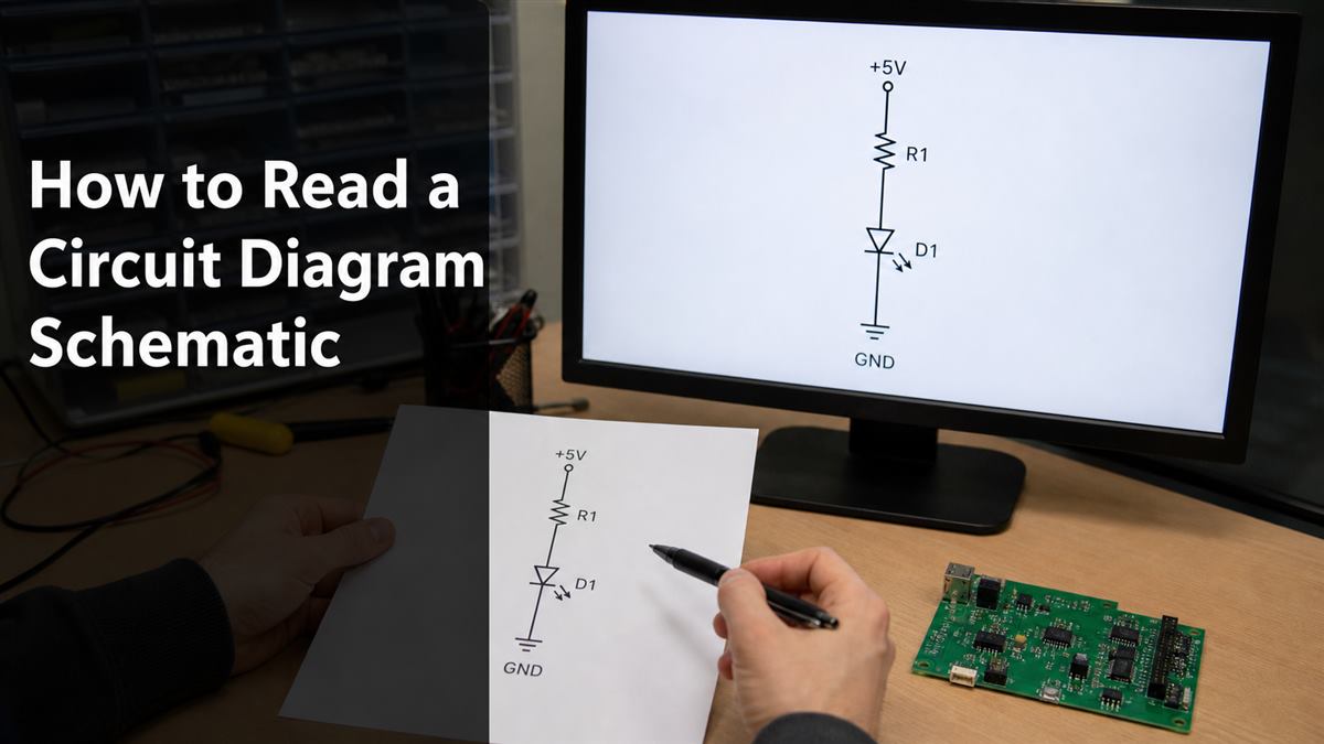
Worked Example: Read a 5 V LED Indicator From Start to Finish
Consider this simple series path:
+5 V -> R1 1 kΩ -> D1 LED -> GNDRead it in the same order you would use on a larger circuit.
1. Identify the boundaries. The source is the +5V rail. The return reference is GND. The output is light from D1.
2. Identify the parts and orientation. R1 is a 1 kΩ resistor. D1 is a polarized LED, so its anode and cathode must match the intended current direction.
3. State the function of each part. The LED converts some electrical energy into light. The resistor limits current; it is not decorative and should not be replaced with a wire.
4. Estimate the expected current. If the LED datasheet gives a forward voltage near 2 V at the intended operating point, Ohm’s law gives:
I = (5 V - 2 V) / 1000 Ω
I = 0.003 A = 3 mA
This is an initial estimate. LED forward voltage changes with device type, current, and temperature. The calculation does not by itself prove brightness, driver capability, or thermal reliability.
5. Predict fault results.
- If D1 is reversed, the LED normally will not light at this voltage.
- If R1 is open, the path is broken and current is approximately zero.
- If R1 is accidentally shorted, current may become excessive and damage the LED or source.
- If the
+5Vrail is missing, neither a good resistor nor a correctly oriented LED can make the circuit work.
You have read this circuit when you can explain the path, the purpose of both parts, the expected current range, the important polarity, and the observations that would support or reject each fault hypothesis.
Follow Nets Across Multi-Page and Hierarchical Schematics
On a multi-page schematic, follow names and hierarchy rather than searching for one long drawn wire. Start with the sheet index or root sheet, identify the block or sheet pin, record the net name exactly, and find the matching label at the destination.
A practical sequence is:
- Read the title block, revision, sheet number, and hierarchy.
- Find the off-page, global, or hierarchical label at the point where the net leaves.
- Record its exact spelling, including suffixes such as
_N,_P,EN, orRESET. - Use the EDA tool’s find or highlight-net command when source files are available.
- At the destination sheet, confirm the receiving pin and the label scope.
- Check for intermediate connectors, series resistors, level translators, or test points.
Do not assume all matching words connect everywhere. In KiCad, local labels, global labels, hierarchical labels, sheet pins, and power symbols have defined scopes and naming rules. Other tools may differ. The source project and tool documentation are more reliable than a screenshot.
Correct the Reading Mistakes That Cause the Most Confusion
| Mistake | Why it fails | Better habit |
| Reading symbol position as physical placement | Schematics prioritize logic; IC pins may be rearranged | Use pin numbers, datasheet, footprint, and PCB layout for physical mapping |
| Memorizing every symbol before reading | It delays practice and still does not explain function | Learn the common set, then look up unfamiliar parts in context |
| Assuming every crossing connects | Many drawings require a junction dot | Check dots, line endings, bridges, and the project legend |
| Treating net labels as comments | Labels may create real electrical connections | Search identical labels and check their scope |
| Assuming all ground symbols mean earth | A circuit can contain several reference and return domains | Identify GND, AGND, DGND, chassis, and earth separately |
| Tracing the whole page at once | Branches and feedback paths quickly become confusing | Trace one source-to-destination path and record expected state |
| Ignoring component values | A 100 Ω and 100 kΩ resistor can give the same symbol a very different role | Read symbol, value, surrounding parts, and datasheet together |
| Jumping from one symptom to one failed part | Several causes can produce the same symptom | List hypotheses and identify evidence that supports or contradicts each |
Prove That You Understand the Schematic
Understanding is demonstrated by predictions, not by recognizing shapes. For the block or path you studied, you should be able to produce all of the following:
- A one-sentence purpose for the block.
- The power source, voltage domain, reference, and return path.
- One complete input-to-output or source-to-load path.
- The role of each component that materially changes that path.
- The expected DC voltage, logic state, waveform type, or operating condition at important nodes.
- A list of unknowns that require a datasheet, note, simulation, or measurement.
- At least two possible fault hypotheses and the observation that would separate them.
- The matching reference designators in the BOM or PCB layout when physical identification matters.
If you cannot do these things, mark the missing point rather than guessing. An honest unknown: U4 pin 7 function requires datasheet is better engineering than a confident story built from symbol position.
Save This Circuit Schematic Reading Checklist
- Read the title block, revision, sheet number, notes, and legend.
- State whether the document is a schematic, wiring diagram, block diagram, or PCB layout.
- Find all incoming power sources and generated voltage rails.
- Identify ground and return domains without assuming they are earth.
- Mark external inputs, outputs, connectors, and loads.
- Divide the drawing into functional blocks.
- Learn or look up unfamiliar symbols, values, and reference designators.
- Check every ambiguous wire crossing for a junction dot or project convention.
- Search matching net labels and confirm local/global/hierarchical scope.
- Choose one path and record source, destination, reference, and expected state.
- Verify IC pin numbers and functions against the exact datasheet and package.
- Predict key node states before simulation or safe measurement.
- Record uncertainties and competing fault hypotheses.
- Map relevant reference designators to the BOM and PCB layout.
- Stop and escalate before energized work on hazardous voltage or stored-energy circuits.
Connect the Schematic to PCB Layout, BOM, and Manufacturing Review
A schematic can be electrically clear and still be incomplete for PCB manufacturing or assembly. The next handoff should connect design intent to physical implementation and production data.
| Handoff item | What it proves or communicates |
| Schematic PDF and source files | Electrical intent, net names, references, and revision |
| BOM with manufacturer part numbers | Which actual components and approved substitutions are intended |
| PCB source or Gerber/ODB++ data | Physical placement, copper, layers, pads, and board geometry |
| NC drill files and stackup notes | Hole data and board construction |
| Pick-and-place/CPL and assembly drawing | Component side, position, rotation, and polarity |
| Programming and test requirements | Firmware, fixtures, test points, limits, and expected behavior |
| Revision note or change list | Which design version the supplier should build |
To continue from logic into physical review, use PCBTRY’s guides on how to design a PCB board for a circuit, how to go from schematic to PCB in KiCad, and how to read PCB layout.
If you want a PCB/PCBA manufacturing review, send the current schematic, Gerber or PCB data, NC drill files, BOM, CPL, stackup, quantity, and test requirements to [email protected]. A manufacturing review can flag file consistency, footprint, assembly, test-access, and DFM questions; it does not replace circuit-design ownership or functional validation.
Frequently Asked Questions About Reading Circuit Schematics
Is a circuit diagram the same as a schematic?
In electronics, the terms are often used interchangeably. A schematic emphasizes symbolic electrical relationships. A wiring diagram usually emphasizes physical wires, terminals, or installation details, so check the document purpose before applying schematic-reading conventions.
What should I read first on a schematic?
Read the title block and notes, then find power sources, ground or return domains, external inputs, and outputs. Divide the drawing into functional blocks before tracing individual signals.
Do I need to memorize every electronic symbol?
No. Memorize the common passive, semiconductor, power, ground, connector, and IC forms. Use the reference designator, value, legend, and datasheet for unfamiliar symbols.
Are identical net labels always connected?
They are connected only within the scope defined by the EDA tool and project. A global label may cross sheets, while a local label may not. Check the source project, hierarchy, and software documentation.
Is ground always zero volts and the same as earth?
Ground is commonly used as the circuit’s reference node, so other voltages are measured relative to it. It is not automatically protective earth, and separate analog, digital, chassis, or isolated grounds may exist.
Can a schematic tell me where a component is on the PCB?
The reference designator links the schematic component to the BOM and PCB layout, but schematic position does not show physical placement. Open the PCB layout or assembly drawing and search the same reference, such as U3 or R17.
How can I get faster at reading schematics?
Practice on small circuits, explain each block in one sentence, trace one path at a time, predict node states, and then compare your prediction with a datasheet, simulation, or safe measurement. Speed comes from repeating the same reasoning method, not from guessing faster.



1 Comment
How to Cross-Check a PCB Schematic Against the Physical Board - thindry pcb manufacturer · 08/26/2026 at 08:16
[…] How to Read a Circuit Diagram Schematic for symbols, nets, and signal flow. […]