




What Does “Testing a PCB” Actually Mean?
To test a PCB properly, first decide what kind of board you have and what you need to prove. An unpopulated bare board, an assembled PCBA, a first prototype and a failed product need different tests. The useful question is not simply “Does it beep?” but “Which failure am I trying to detect, and what result would prove the board passed?”
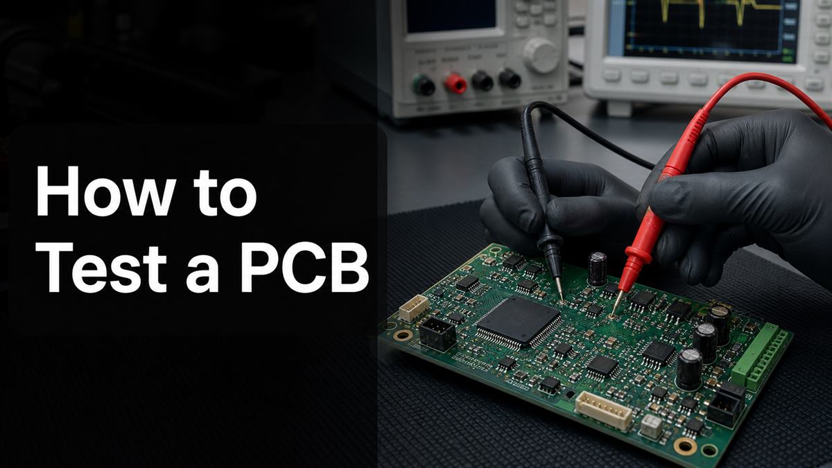
A fabricated bare PCB can be checked for open and shorted copper networks before components are fitted. That electrical test does not prove that solder mask, hole geometry, component placement or final operation is correct. Once components are assembled, inspection and electrical checks can find assembly defects, while functional testing asks whether the board performs its intended job.
| Board state | Main question | Useful evidence | What it does not prove |
| Bare PCB | Do the copper networks match the design? | Continuity/isolation e-test, fabrication inspection | Assembly quality or product function |
| Unpowered PCBA | Is assembly safe enough for first power? | Visual inspection, polarity, resistance and continuity checks | Correct powered behavior |
| Powered prototype | Do the rails, reset, clock and functional blocks behave as designed? | Current, voltage, waveform and functional results | Production consistency or long-term reliability |
| Production PCBA | Can each unit meet documented acceptance limits? | AOI/X-ray, ICT or flying probe, programming and FCT records | Every possible field condition |
What Should You Know Before Touching the Board?
Before testing, identify the power source, expected voltages, ground reference, board revision and known hazard areas. A meter is only useful when you know what its probes are connected across and what reading the design should produce.
Collect the schematic, PCB assembly drawing, BOM, connector pinout and any test-point map. If a known-good board exists, record comparable readings under the same power, load and meter settings. A photograph of both sides before work also preserves evidence that may disappear after rework.
- Disconnect external power and batteries before continuity, resistance or diode-mode checks.
- Allow charged capacitors to discharge using the product’s approved method.
- Use ESD controls when handling sensitive assemblies.
- Do not probe mains, non-isolated supplies, high-voltage sections or high-energy battery systems unless you are trained and have correctly rated equipment.
- Know whether an ordinary oscilloscope probe ground is tied to protective earth before clipping it to the board.
If the circuit has an unknown energy source or the ground reference is uncertain, stop. That is an equipment and safety problem, not a reason to improvise with a probe.
Which Tools Do You Need to Test a PCB?
Use the simplest tool that can answer the current question, then move to a more capable tool only when the result demands it. A magnifier often finds a solder bridge faster than a meter; a meter finds a missing rail but cannot show whether a clock is oscillating correctly.
| Tool | Best use | Typical finding | Blind spot |
| Light and magnification | Surface inspection | Bridge, crack, reversed part, contamination | Hidden joints and electrical behavior |
| Digital multimeter | Continuity, resistance, diode checks and DC rails | Open path, unexpected rail resistance, missing voltage | Fast waveforms, protocols and full function |
| Current-limited supply | Controlled first power-up | Unexpected current draw or rail collapse | Exact fault location |
| Oscilloscope | Clock, reset, ripple and changing signals | Missing waveform, distortion or timing problem | Wrong probe setup can create misleading results |
| Logic analyzer | Digital timing and protocol activity | Missing or malformed transactions | Analog integrity and power faults |
| Thermal camera | Temperature pattern under controlled power | Unexpected hot area | Heat identifies a symptom, not automatically the root cause |
| ICT/flying probe/FCT fixture | Repeatable production screening | Documented unit-level pass/fail | Coverage is limited by access, program and test limits |
What Is the Correct PCB Testing Order?
The correct order moves from low-risk observation to controlled electrical testing. Each stage earns permission for the next one. Applying full power first can turn a misplaced component or solder bridge into damaged copper and lost evidence.
- Step 1: Define the expected behavior. Write down input voltage, expected idle current, rail voltages, required outputs and the board revision.
- Step 2: Inspect without power. Compare component orientation, soldering and connectors with the assembly data.
- Step 3: Check unpowered rails. Measure resistance to ground and investigate unexpected readings without treating one beep as a verdict.
- Step 4: Check critical continuity. Verify suspected opens from one known endpoint to another.
- Step 5: Apply controlled power. Use the correct polarity and a justified current limit.
- Step 6: Verify power rails. Follow power from the connector through protection and regulation.
- Step 7: Check startup conditions. Confirm reset, clock, enable and programming state.
- Step 8: Test one functional block at a time. Trace the failed function from input to output.
- Step 9: Record pass/fail evidence. Save conditions, readings, limits and unit identity.
This order is a diagnostic tree, not a ritual. If a stage fails, stop and isolate that failure rather than continuing to collect unrelated readings.
How Do You Inspect a PCB Before Applying Power?
Inspect the highest-risk areas first: the power input, polarized components, fine-pitch packages, connectors and any location that was reworked. Use the assembly drawing and BOM instead of judging only by appearance.
- Confirm the board revision and component reference designators.
- Check diode, LED, electrolytic capacitor and IC orientation.
- Look for solder bridges, unsoldered pins, tombstoned passives and solder balls.
- Inspect lifted pads, cut traces, damaged vias and cracked components.
- Check that connectors are the correct part and installed in the intended orientation.
- Look for conductive debris, corrosion, moisture and residue where cleanliness matters.
A dark mark is evidence to examine, not proof that a component failed. Flux residue can look burned, while a damaged semiconductor may look perfect. Mark suspicious locations and confirm them with the next appropriate test.
For more examples of visible and electrical warning signs, see how to tell if a PCB is damaged.
How Do You Check for Shorts Without Power?
Check for shorts by measuring resistance between each power rail and its intended return while the board is disconnected and discharged. Start with the highest-level rails, then divide the circuit only if a reading is unexpected.
- Step 1: Confirm that all power sources are removed and capacitors are discharged.
- Step 2: Put the black lead in COM and the red lead in the voltage/resistance jack, not the current jack.
- Step 3: Briefly touch the probes together to understand lead resistance and meter behavior.
- Step 4: Measure rail-to-ground resistance in both probe directions and watch whether the value changes as capacitors charge from the meter.
- Step 5: Compare the reading with the schematic, design expectation or a known-good board measured the same way.
A continuity beep means the resistance is below that meter’s audible threshold. It does not, by itself, prove a short circuit. Low-voltage processor rails, heater loads, coils and many parallel components can have low resistance by design. A reading that rises after probe contact may be capacitor charging rather than a fault.
If the rail is genuinely abnormal, isolate branches at removable links, fuses, inductors or zero-ohm jumpers where the design permits. Do not randomly remove parts; each isolation step should test one hypothesis and preserve the original failure evidence.
How Do You Test Continuity and Suspected Broken Traces?
Test continuity between two known endpoints on the same net, not by sweeping the board until the meter beeps. The schematic or PCB data tells you which pads should be connected and which nearby pads must remain isolated.
- Step 1: De-energize and discharge the board.
- Step 2: Place one probe at the source endpoint and the other at the destination endpoint.
- Step 3: Read the displayed resistance rather than relying only on sound.
- Step 4: Gently flex only connectors or cables intended to move while watching for an intermittent reading.
- Step 5: Check isolation to adjacent nets if a bridge is possible.
In-circuit paths can run through resistors, protection devices or IC structures, so a resistance reading may not equal the copper trace resistance. When a result is ambiguous, compare shorter sections of the same net or isolate one end of the component if that can be done without creating new damage.
How Do You Power Up a PCB Without Turning a Small Fault Into Damage?
Use the specified input voltage, correct polarity and a current limit based on the board’s expected startup behavior. The purpose of the limit is to provide evidence and time to stop, not to guess a universal “safe” current.
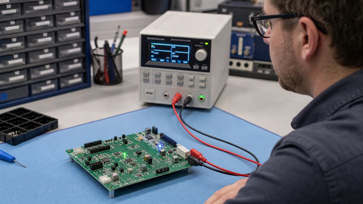
- Step 1: Verify the supply leads at the board connector before connecting them.
- Step 2: Set the intended voltage and a justified current limit while the output is off.
- Step 3: Connect the board, keep probes clear of adjacent pins and enable the output.
- Step 4: Watch both voltage and current. If voltage collapses into current limit or current differs sharply from the expected startup profile, switch off.
- Step 5: Check for unexpected heating only under controlled conditions. Never use touch on hazardous circuits.
Some boards have legitimate inrush current from bulk capacitors, motors, radios or displays. That is why the acceptance plan needs both a peak behavior and a settled behavior where relevant. A current limit set below normal startup demand can make a good board appear faulty.
How Do You Check Power Rails and Regulators?
Trace power in its real order: connector, protection, switching element, regulator input, regulator output and load. Measuring only one convenient test point can miss a reversed protection device, blown fuse, disabled regulator or collapsed downstream rail.
| Check | Expected evidence | If it fails |
| Input connector | Correct polarity and specified input voltage | Check cable, connector and source |
| After protection | Input passes through fuse/reverse-polarity/TVS path as designed | Inspect protection devices and orientation |
| Regulator input | Voltage within the regulator’s documented operating conditions | Trace upstream drop or enable path |
| Regulator enable | Logic state matches the design sequence | Check controller, pull resistor or sequencing signal |
| Regulator output | Rail reaches its design target under the stated load | Separate regulator, shorted load and current-limit hypotheses |
| Load-side test point | Rail reaches the consuming device without excessive drop | Inspect vias, connectors, filters and narrow paths |
Use the circuit ground specified for the measurement. If the rail is switched, isolated, negative or floating, the nearest exposed metal is not automatically the correct reference.
How Do You Trace a Board That Powers Up but Does Not Work?
When all main rails are present, stop measuring random components and follow the failed function as blocks. A digital controller board commonly needs valid power, released reset, a working clock, correct boot configuration, firmware and an intact input/output path.
- Step 1: Define the symptom precisely. “No output” is more useful when stated as the connector, channel, load and operating command that fail.
- Step 2: Confirm prerequisites. Check relevant rails, enable signals, reset and clock.
- Step 3: Confirm the command reaches the block. Use a scope or logic analyzer with the correct reference and bandwidth.
- Step 4: Check the block output. Compare the observed signal with the schematic, datasheet and expected operating state.
- Step 5: Move one boundary at a time. The last correct node and first incorrect node define the smaller fault region.
For fast signals, long oscilloscope ground leads can add ringing that is not present at the test point. Use a short ground connection or a suitable differential/isolation probe when the circuit requires it. Never defeat an oscilloscope’s protective earth to make a ground-referenced probe “float.”
If you need to rebuild the functional path from the drawing, this guide to reading a circuit diagram schematic explains how to follow power, nets and signal flow.
How Do You Test Components Without Misreading the Rest of the Circuit?
In-circuit component measurements include every parallel path connected to the probes. Use them to find differences and suspicious behavior, not to assume the displayed value is the isolated component value.
- Resistors: a parallel path can make the reading lower than the marked value. Lift one end only when the diagnosis justifies rework.
- Capacitors: resistance mode may show a changing value as the part charges. Capacitance and ESR measurements can also be distorted by the surrounding circuit.
- Diodes and junctions: diode mode is useful for comparing polarity and junction behavior, but other semiconductor paths can appear in parallel.
- Inductors and transformer windings: low DC resistance may be normal. Continuity does not prove inductance, insulation or behavior at operating frequency.
- ICs: a multimeter cannot prove firmware execution, logic timing or analog performance. Compare rail resistance and diode signatures with known-good evidence when available.
A part that measures differently deserves investigation; it is not automatically the root cause. Confirm the operating condition, isolate the path when necessary, replace one variable at a time and repeat the original failure test.
Which Production Test Method Fits Bare Boards, Prototypes and Volume Builds?
Choose production tests by defect target, access, volume, fixture economics and escape risk. No single method replaces the others because seeing a joint, measuring a node and running the product answer different questions.
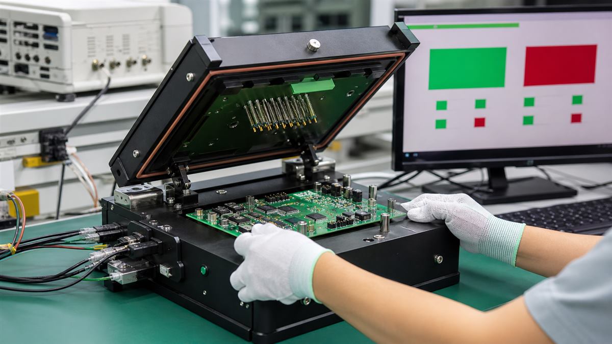
| Method | Best at finding | Common blind spot | Typical fit |
| Bare-board e-test | Open and shorted copper networks | Assembly and product function | Fabricated unpopulated boards |
| AOI | Visible placement and solder features | Hidden joints and electrical function | Fast process inspection after assembly |
| X-ray | Hidden solder-joint geometry and alignment | Many electrical and firmware faults | BGA/QFN and other hidden-joint risks |
| Flying probe | Programmable node checks without a dedicated bed-of-nails fixture | Full application behavior; cycle time | Prototypes and changing designs |
| ICT | Repeatable node/component-oriented manufacturing checks | Firmware and complete system behavior | Stable designs with sufficient test access |
| Boundary scan | Supported digital interconnects with limited physical access | Unsupported devices and analog behavior | Dense digital assemblies designed for JTAG |
| Functional test | Application inputs, outputs and operating sequence | May report failure without locating the defective part | Final product or subassembly verification |
For a deeper comparison of production methods, see ICT and functional test verification and how in-circuit testing works.
How Do You Decide Whether the PCB Passed?
A PCB passes only when it meets written limits under written test conditions. “It powered on,” “the LED lit” and “the meter beeped” are observations; they are not complete acceptance criteria.
| Record field | Example of useful evidence |
| Unit identity | Board revision, serial/lot and assembly version |
| Test condition | Input source, load, firmware, temperature and fixture revision |
| Test point or function | Rail name, connector pin, signal name or output channel |
| Expected result | Design target or approved min/max limit |
| Measured result | Value, waveform, event or functional response |
| Instrument | Meter/scope/fixture identity and relevant setup |
| Decision | Pass, fail, not tested or inconclusive |
| Follow-up | Failure code, isolation result, rework and retest result |
An inconclusive result is not a pass. If the test cannot reach a node, the load is not representative or the expected waveform is unknown, record the gap and choose another method. After repair, repeat the original failed test and any neighboring checks that the rework could affect. Guidance on repair decisions is available in how to fix a circuit board.
What Test Information Should You Send to a PCB/PCBA Manufacturer?
Send enough design and acceptance information for the manufacturer to build a repeatable test, not just the instruction “test every board.” The test method, fixture and quotation depend on what defects must be found and what access the design provides.
- Gerber or ODB++ data and fabrication drawing for the correct revision.
- BOM with manufacturer part numbers and approved substitution rules.
- CPL/pick-and-place data and assembly drawings.
- Schematic, connector pinout and test-point map.
- Programming files, firmware version and programming procedure.
- Input power, safe current limits, loads and required accessories.
- Test sequence with expected values, tolerances and timing conditions.
- Fixture interface, mating connectors and golden-sample policy where applicable.
- Required report, traceability, failure codes and retest rules.
For PCB fabrication, assembly or a testability review, send the current Gerber/ODB++, BOM, CPL, schematic and test limits to [email protected]. The useful starting request is not “Can you test it?” but “Which defects does this plan cover, what remains untested, and what design access is missing?”
Frequently Asked Questions
Can you test a PCB with only a multimeter?
You can perform useful continuity, resistance, diode and DC-voltage checks with a multimeter. That is enough to find many opens, obvious shorts and missing power rails. It cannot prove clock quality, protocol timing, firmware behavior, hidden solder-joint integrity or full product function. Use the meter as one layer in a test plan, not as a universal pass certificate.
Does a continuity beep mean the PCB has a short?
No. The beep only means the measured resistance is below the meter’s continuity threshold. A legitimate low-resistance load, coil, low-voltage rail or capacitor-charging path can produce a beep. Read the displayed resistance, measure in both directions and compare with the schematic or a known-good board before declaring a short.
Can resistance be measured while the PCB is powered?
No. Resistance and continuity modes apply their own small test signal and should be used on a de-energized, discharged circuit. External voltage can produce false readings or damage the meter. When the board is powered, use the correctly rated voltage, current or waveform measurement method instead.
Why does a power-to-ground reading start low and then rise?
The meter may be charging capacitors connected across the rail, so the apparent resistance changes with time. Reverse the probes and repeat under the same conditions, then compare with the circuit design. A changing reading is useful evidence, but it neither proves nor rules out a short by itself.
What should you test first when a new PCB does not start?
First switch off and inspect component orientation, solder bridges and the power input path. Then check unpowered rail resistance. If those checks are reasonable, use controlled power and verify the input, regulated rails, enable signals, reset and clock in that order. This sequence separates a power problem from a boot or functional problem.
How do you test a PCB without a schematic?
Begin with safe visual inspection, connector labels, component datasheets and obvious power paths. Compare with an identical known-good board if available. You can identify gross shorts and missing rails, but confidence is lower because expected connections and values are unknown. Avoid powered probing on unfamiliar high-energy sections and record results as provisional.
What is the difference between testing a PCB and a PCBA?
A PCB is the unpopulated printed board, so testing mainly checks copper-network continuity, isolation and fabrication features. A PCBA includes components and solder joints, so inspection, component-oriented electrical tests, programming and functional operation become relevant. Passing bare-board e-test does not prove that the assembled product works.
Should every production board receive functional testing?
The required coverage depends on product risk, design maturity, process capability, test access and customer requirements. Functional testing is often valuable because it verifies application behavior, but it may not isolate the root cause and cannot replace every structural inspection. Define the defect risks and acceptance evidence first, then select the test combination with the manufacturer.



0 Comments