




What Is PCB Solder Mask?
PCB solder mask is the protective polymer layer that covers most of the copper on a printed circuit board. It is usually green, but it can also be black, white, blue, red, yellow or other colors. The copper pads that need soldering are left exposed through solder mask openings.
Solder mask helps prevent solder bridges, protects copper from oxidation, improves board handling and makes the PCB easier to inspect. It is not the same as the copper layer, silkscreen or surface finish.
What Solder Mask Actually Does
| Function | Why it matters | Limit |
|---|---|---|
| Separates solderable pads | Reduces solder bridge risk | Cannot fix badly spaced pads |
| Protects copper | Slows oxidation and contamination | Exposed pads still need surface finish |
| Improves handling | Protects traces during assembly | Can be scratched or damaged |
| Supports inspection | Contrasts pads, traces and silkscreen | Dark colors can reduce visual contrast |
Solder Mask Openings and Clearance
A solder mask opening is an area where the mask is removed so a pad can be soldered or contacted. The opening is normally slightly larger than the copper pad to account for manufacturing tolerance.
If the opening is too small, solderability can suffer. If it is too large, nearby copper may be exposed and solder bridge risk may increase. Fine-pitch components need careful solder mask clearance.
Solder Mask Defined vs Non-Solder Mask Defined Pads
Most standard pads are non-solder mask defined, meaning the copper pad defines the solderable area. Solder mask defined pads use the mask opening to define the pad area. This can matter for BGA and fine-pitch parts.
Do not switch pad definition casually. It affects assembly and should match component package guidance and manufacturer capability.
PCB Solder Mask Colors
Green solder mask is the most common because it is familiar, stable and easy to inspect. Other colors are possible, but they may affect lead time, cost, visual inspection or marking contrast.
| Color | Typical reason to choose | Check |
|---|---|---|
| Green | Standard production and easy inspection | Best default for most boards |
| Black | Product appearance | Can make inspection harder |
| White | LED reflection or appearance | Can show contamination and process marks |
| Blue or red | Branding or revision separation | Confirm availability and lead time |
Solder Mask Thickness and Reliability
Solder mask thickness affects coverage, edge definition and clearance around pads. Very thick or uneven mask can create issues around fine-pitch parts, while poor coverage can expose copper where it should be protected.
For special high-voltage, high-current, LED or harsh-environment boards, discuss solder mask requirements with the manufacturer before fabrication.
Common Solder Mask Defects
| Defect | What it means | Why it matters |
|---|---|---|
| Mask misregistration | Opening shifted from pad | Can reduce solderable area or expose copper |
| Mask bridge missing | No mask between fine pads | Increases solder bridge risk |
| Pinholes | Tiny uncovered spots | May expose copper to contamination |
| Peeling | Mask adhesion failure | Reliability and handling concern |
| Wrong opening | Pad or test area not exposed correctly | Assembly or test failure |
Where Solder Mask Should Be Removed
Solder mask should be opened on component pads, test points, connector contacts, fiducials when required and special exposed copper features. It should remain over copper traces that do not need soldering or contact.
For test points, make sure the opening is large enough for probes. For thermal pads or exposed copper areas, clearly state whether they should be solderable, bare copper, surface finished or mask covered.
DFM Checks Before Fabrication
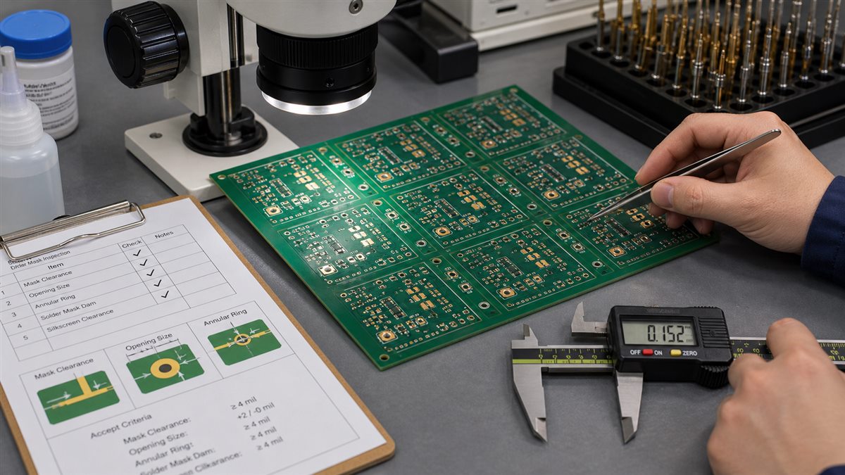
- Check solder mask clearance around fine-pitch pads.
- Confirm minimum solder mask bridge capability.
- Review BGA and QFN pad definition.
- Confirm mask openings for test points and connectors.
- Check color availability and inspection impact.
- Confirm any special high-voltage or LED requirements.
FAQ
Why is PCB solder mask usually green?
Green is common because it is stable, widely available and easy to inspect. Other colors are possible but may affect inspection and lead time.
Is solder mask an insulator?
It provides insulation over copper areas, but it should not be treated as the only safety barrier for high-voltage design. Clearance and creepage rules still matter.
Can solder mask cover vias?
Yes, vias can be tented or covered depending on design needs. The requirement should be stated clearly in fabrication notes.
What is solder mask clearance?
It is the gap or expansion between the copper pad and solder mask opening. It allows manufacturing tolerance and proper solderability.
Confirm Solder Mask Requirements Before Ordering
PCB solder mask affects solderability, inspection, reliability and appearance. Before fabrication, check openings, clearance, color, via tenting, test points and fine-pitch features.
PCBtry can review your PCB fabrication files and solder mask requirements before production. Send Gerber files, fabrication notes and any special solder mask color, opening or via tenting requirements through the contact page.



0 Comments