




PCB etching is a subtractive process: a resist protects the copper pattern you want to keep while an etching process removes the exposed copper. It can be a useful learning exercise or a way to make a simple prototype, but it is not a shortcut to every type of printed circuit board. The board, resist, documented etchant, workspace controls, and waste route all affect whether an in-house process is appropriate.
Should You Etch a PCB Board Yourself?
Start with the board requirement, not the chemical. A simple, low-risk, single-sided learning board with generous spacing may be a reasonable candidate for an in-house process if you have suitable training, ventilation, PPE, a documented etchant process, and an approved route for chemical waste. A board that needs plated through holes, multilayer registration, tight geometry, controlled impedance, a qualified finish, or repeatable production controls belongs with a capable PCB fabricator.
Etching makes a copper pattern; it does not create all of the features needed for a production board. Before committing, compare the design need with PCB prototyping and decide whether a manufactured prototype will provide a more useful result.
What PCB Etching Removes and What the Resist Protects
Copper-clad laminate starts with copper foil on an insulating base. Artwork and resist identify the areas that should remain as traces, pads, or copper areas. The etching stage removes copper that is not protected by the resist. Afterward, the remaining resist is removed and the copper pattern is inspected.
This is why image quality and surface preparation matter. A gap in the resist can expose copper that should remain. A bridge in the resist can leave copper where clearance was intended. The process cannot correct an inaccurate layout or replace design-rule checking before fabrication.
Safety and Chemical Boundaries Before You Start
Use the safety data sheet and instructions for the exact etchant and related materials you have selected. They define required PPE, ventilation, compatible containers, first-aid measures, storage, rinse requirements, and waste handling. Do not substitute a recipe found online, combine household chemicals, or pour spent solution into a drain.
Work with the board unpowered. Prepare a stable work surface, protect nearby equipment from splashes, and keep food, drinks, and unrelated tools away. If the chemical identity, container, condition, ventilation, or local disposal route is uncertain, stop before opening it and obtain the relevant documentation or local hazardous-waste guidance.
Choose an In-House Etch or a Fabricated PCB
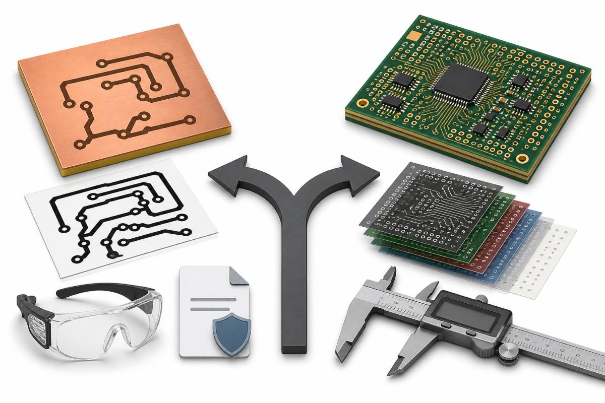
| Need | In-house etching may fit | Use a PCB fabricator when |
|---|---|---|
| Learning or a simple proof of concept | Single-sided, generous-clearance work with a documented safe process. | You need a repeatable result for multiple assemblies. |
| Holes and interconnects | Non-plated holes may be acceptable for a limited experiment. | Plated through holes, vias, or reliable multilayer interconnects are required. |
| Geometry and performance | Features are deliberately conservative for the available method. | Fine pitch, controlled impedance, dense routing, RF performance, or production DFM matters. |
| Material and finish | The material is known and compatible with the documented process. | You need controlled stackup, specified copper, surface finish, testing, or certification evidence. |
| Chemical handling | You have SDS-led controls and an approved waste route. | You cannot verify safe handling, storage, or disposal. |
If the board is headed to manufacturing, create clean production files rather than relying on a hand-made pattern. PCBtry’s Gerber-file guide explains the file handoff used by fabricators.
Prepare the Artwork, Copper-Clad Board and Resist
Check the artwork before any material is exposed. Confirm that the intended copper, clearances, pads, text orientation, and hole references match the schematic and the assembly plan. Treat the final artwork as a controlled input: changing it after resist transfer makes it harder to tell whether a defect came from the design or the process.
Prepare the copper-clad board only with the method compatible with the material and resist system. The aim is a clean, dry surface that lets the selected resist form a continuous protective pattern. Do not assume every abrasive, solvent, marker, film, or transfer method is compatible. Follow the documented instructions for the resist system.
How to Etch a PCB Board: Process Overview
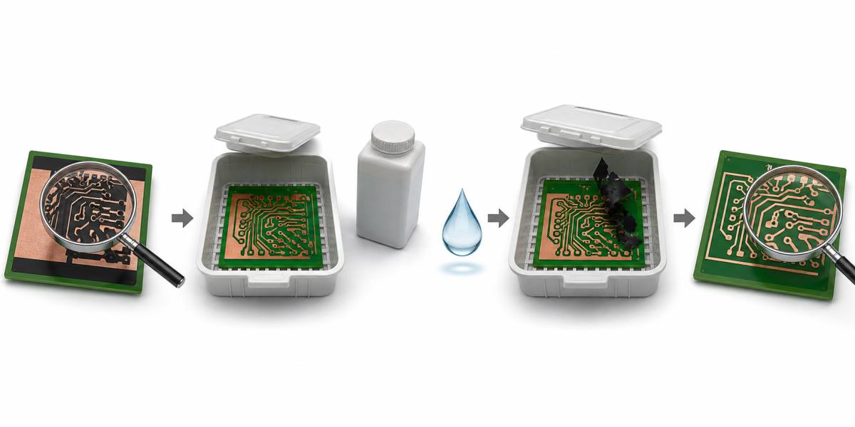
- Plan the process. Confirm the board is an appropriate candidate, identify the exact materials, and review the SDS and waste route.
- Verify artwork and resist coverage. Inspect the pattern before etching. Look for gaps, pinholes, lifted edges, and unintended bridges.
- Use the documented etchant process. Follow the manufacturer instructions for the selected product, including container, handling, temperature, agitation, exposure, and endpoint guidance. Do not improvise concentrations or timings.
- Watch the board, not a generic timer. When exposed copper has been removed according to the process instructions, end the process using the documented rinse or stop step.
- Keep solution and waste controlled. Do not move spent liquid into food containers, drains, or ordinary trash. Label it and use the approved local disposal route.
- Strip the resist only with a compatible documented method. Then clean and dry the board before inspection.
Rinse, Strip Resist and Inspect the Copper Pattern
After the documented stop/rinse step and resist stripping, inspect under good light and magnification. Check that unwanted copper is absent, traces are continuous, clearances are open, pads are intact, and there are no pinholes, copper whiskers, residue films, or damaged areas. A visual check does not prove electrical performance, so use continuity or other appropriate verification before attaching valuable components.
If residue remains, use only a material-compatible cleaning process. The broader PCB cleaning guide is useful for contamination decisions, but it does not replace the etchant or resist documentation.
Review the Pattern Before You Populate the Board
Etching is only one manufacturing step. Before soldering components, compare the finished copper pattern with the approved artwork and schematic. Confirm orientation markers, connector pin order, power and ground paths, isolation areas, and any features that are difficult to correct after components are installed. This review is especially important when the board is a first prototype, because an apparent etch defect may actually be an artwork or library error.
Use a staged verification approach. First, confirm that expected copper is present and unwanted copper is absent. Next, check continuity where the design expects a connection and check isolation where the design expects separation. Then decide whether the board is suitable for low-risk assembly or should be remade. Do not use the board for high-value hardware, safety-critical equipment, or a reliability claim until the relevant design and manufacturing verification has been completed.
A fabricated prototype gives you different controls: production-file review, manufacturing feedback, controlled materials, and testing options. PCBtry’s PCB manufacturing guides can help when the next step is a manufacturable prototype rather than another home-etch iteration.
Troubleshooting: Incomplete Etch, Resist Failure and Stop Conditions
Exposed copper remains: do not assume the answer is more time or a stronger mixture. Check the artwork, resist coverage, chemical identity and condition, and documented process endpoint. Unwanted copper disappeared: inspect for resist gaps, edge lift, handling damage, or an artwork error. Fine features look uneven: treat that as a process-capability limit and consider a fabricated board rather than repeating a risky chemical step.
Stop if the board has unknown materials, the chemical is unidentified, the work area lacks the required controls, the board needs plated holes or qualified performance, or waste handling cannot be verified. The safest next action can be to order a prototype rather than continue the home process.
Keep a Simple Process Record
For a learning build, record the board material, artwork revision, resist system, etchant product name, date, inspection observations, and the waste route used. This is not a production certificate. It is a practical way to avoid repeating an unknown combination when a result is poor, and it makes the next prototype review more useful. Keep the record with the design files, not on an unlabelled container or loose note beside chemicals.
When an etched board fails inspection, preserve the artwork and a clear photograph before stripping or reworking it. Compare the issue against the original copper pattern: a repeatable location can point to artwork or resist coverage, while random damage may point to handling or process control. If the cause remains uncertain, do not infer it from one board; choose a fabricated prototype or seek qualified process advice.
Published Engineering Scenario: Why Process Variables Matter
Problem: a public PCB fabrication reference explains that copper pattern etching removes copper not protected by a suitable metal or polymer resist, and that resist and etchant chemistry must be compatible. The engineering problem is not merely removing copper: the protected pattern must survive the relevant process.
Treatment: the source describes selecting an etchant compatible with the resist material and then fully removing resist and rinsing as part of the manufacturing sequence. This is a process-control example, not a home-lab test result or a recommendation for a particular chemical.
Reader lesson: treat the resist, board, chemical, and inspection method as a matched system. If compatibility is not documented, do not assume a method works because it worked on a different board.
PCB Etching Checklist
- Board requirement evaluated against in-house limits.
- Artwork checked against schematic and intended copper pattern.
- Exact resist and etchant identified.
- SDS and product instructions reviewed.
- PPE, ventilation, compatible container, and workspace controls ready.
- Waste route confirmed before chemicals are opened.
- Board unpowered and surface prepared by the compatible method.
- Resist coverage checked for gaps and bridges.
- Etching performed only by the documented product process.
- Rinse/stop and resist-strip steps followed as documented.
- Copper pattern inspected under good light and magnification.
- Board kept out of service until dry and appropriately verified.
FAQs About Etching a PCB Board
What does PCB etching do?
It selectively removes exposed copper from copper-clad laminate while resist protects the intended pattern.
Can I etch a PCB board at home?
Only when the board is simple enough and you have a documented safe process, suitable controls, and an approved waste route.
Is home etching suitable for plated through holes?
No. Etching patterns copper; plated-hole reliability requires additional controlled fabrication processes.
Which etchant should I use?
Choose only a product whose documentation covers its use with your board and resist; follow its SDS and instructions rather than a universal recipe.
How long does PCB etching take?
There is no safe universal time. Use the endpoint guidance for the exact documented process.
Why did my traces disappear?
Check for resist gaps, lifted edges, artwork errors, and process compatibility before trying again.
Can I pour used PCB etchant down the drain?
No. Use the product guidance and your local hazardous-waste route.
How do I know etching is complete?
Use the documented endpoint and inspect for unwanted copper, open clearances, and intact traces.
Do I need to clean the board after etching?
Yes, only with compatible documented rinse, resist-strip, and drying steps before inspection.
When should I order a PCB instead?
Order one when the design needs fine geometry, plated holes, multilayers, controlled performance, repeatability, or qualified manufacturing evidence.



0 Comments