





Anyone comparing Altium Designer with SOLIDWORKS PCB in 2026 should begin with one important fact: SOLIDWORKS PCB is now an end-of-life product.
According to the official SOLIDWORKS 2023 release notes, SOLIDWORKS PCB 2023 SP3 was the last supported release of both SOLIDWORKS PCB and SOLIDWORKS PCB Connector. Altium Designer, meanwhile, remains under active development. (files.solidworks.com)
This changes the purpose of the comparison. Altium Designer and SOLIDWORKS PCB are no longer two actively developed platforms competing for the same new customers.
For a new project, the practical question is whether Altium Designer meets the company’s technical, collaboration, and manufacturing requirements. For an existing SOLIDWORKS PCB project, the priority is to preserve the legacy design environment, establish a migration plan, and verify that converted manufacturing data still represents the approved board.
The short answer is:
- For new PCB designs: SOLIDWORKS PCB should not be selected as a long-term ECAD platform because it is no longer supported.
- For legacy designs: Existing SOLIDWORKS PCB projects may still be maintained if the required software, licenses, libraries, and compatible operating environment remain available.
- For migration: Altium provides a documented path for transferring SOLIDWORKS PCB projects, board files, libraries, and design rules.
- For companies using SOLIDWORKS mechanical CAD: Altium MCAD CoDesigner provides a current ECAD–MCAD collaboration workflow without requiring SOLIDWORKS PCB.
Quick Comparison: Altium Designer vs. SOLIDWORKS PCB
| Category | Altium Designer | SOLIDWORKS PCB |
|---|---|---|
| Product status | Actively developed | End-of-life |
| Supported releases | Current releases remain available | Version 2023 SP3 was the final supported release |
| Best use today | New PCB development and legacy project migration | Temporary maintenance of existing projects |
| Schematic and PCB design | Integrated professional ECAD environment | Available in the final legacy release |
| Routing and design rules | Current routing, constraint, and verification workflows | Limited to the capabilities of the final release |
| High-speed PCB design | Current impedance, differential-pair, length-tuning, and signal-path tools | Legacy high-speed feature set |
| Rigid-flex PCB design | Current rigid-flex design environment | Existing legacy capabilities are no longer being developed |
| Component management | File-based, database, and Workspace-managed options | Legacy library and component-management workflows |
| SOLIDWORKS integration | Available through Altium MCAD CoDesigner | Originally provided through SOLIDWORKS PCB Services and PCB Connector |
| Manufacturing outputs | Gerber, Gerber X2, NC Drill, ODB++, IPC-2581, drawings, reports, and other outputs | Production outputs depend on the installed legacy environment |
| Recommended for new projects | Yes, subject to technical and commercial evaluation | No |

End-of-life status does not mean that every installed copy of SOLIDWORKS PCB has stopped working. A maintained installation may continue to open and edit existing projects.
The concern is long-term reliability. Future operating-system compatibility, defect correction, software restoration, license availability, and integration with newer engineering systems may become increasingly difficult to manage.
What Was SOLIDWORKS PCB?
SOLIDWORKS PCB, formerly known as PCBWorks, was a PCB design application integrated with the SOLIDWORKS 3D mechanical design environment.
Its collaboration system allowed electrical and mechanical engineers to exchange PCB changes through a shared repository. An electrical engineer could push a board update to the repository, while a mechanical engineer could pull the update into SOLIDWORKS, evaluate the mechanical impact, make changes, and return those changes to the electrical designer.
SOLIDWORKS PCB Services managed the shared repository. SOLIDWORKS PCB Connector allowed compatible Altium Designer users to participate in the collaboration workflow. (help.solidworks.com)
This approach addressed a common product-development challenge: the PCB and enclosure often evolve at the same time.
Changes to any of the following can affect both teams:
- Board outline
- Mounting-hole locations
- Connector placement
- Component height
- Heat-sink position
- Enclosure walls
- Mechanical keepouts
- Cable access
- User-interface components
- Thermal solutions
A structured ECAD–MCAD workflow can make these changes easier to track than repeatedly exchanging unrelated files by email.
However, the original SOLIDWORKS PCB collaboration environment is tied to an end-of-life product. Companies that still rely on it should preserve the complete environment while preparing a controlled migration plan.

What Is Altium Designer?
Altium Designer is a professional ECAD platform that combines schematic capture, PCB layout, component management, design rules, 3D board visualization, manufacturing documentation, and project output generation.
Depending on the product edition, connected services, license, and installed extensions, Altium Designer can support:
- Hierarchical schematic design
- Interactive PCB routing
- Differential-pair routing
- Length matching
- Controlled-impedance design
- HDI design
- Rigid-flex design
- Multi-board projects
- 3D PCB visualization
- Component library management
- BOM preparation
- ECAD–MCAD collaboration
- Manufacturing documentation
- Managed project releases
Because software editions and subscription packages can change, companies should confirm current feature availability directly with Altium before purchasing a license.
From a PCB supplier’s perspective, one practical benefit is the ability to organize fabrication and assembly deliverables through an Output Job file.
An Output Job can help a design team generate a consistent release package instead of relying on an engineer to remember every export type and setting for each revision.
Why Product Status Matters More Than a Feature Checklist
Many older Altium Designer vs. SOLIDWORKS PCB comparisons focus on user interfaces, routing tools, library features, and license prices.
That approach is no longer sufficient.
Even if a discontinued application contains the features needed for a particular board, a company must consider whether the complete design environment can still be maintained over the expected life of the product.
Important questions include:
- Can the software be installed again if the existing workstation fails?
- Will it remain compatible with future operating systems?
- Can replacement engineers obtain a supported installation?
- Will software defects continue to be corrected?
- Can the company restore all libraries and database connections?
- Will newer mechanical tools continue to communicate with it?
- Can an old production revision be reproduced accurately several years later?
- Are installation files and license records properly archived?
Maintaining SOLIDWORKS PCB may be reasonable for a stable legacy product that requires only minor revisions. It is much harder to justify for a new commercial platform expected to remain in development for many years.
Schematic Capture and PCB Layout
Both Altium Designer and SOLIDWORKS PCB provide schematic capture and PCB layout functions.
The main difference today is not whether both applications can place components or route tracks. The difference is that Altium Designer continues to evolve, while SOLIDWORKS PCB is fixed at the capabilities of its final release.
For a new design, an actively maintained platform provides a more sustainable foundation for:
- Library management
- Design-rule development
- High-speed constraints
- Mechanical collaboration
- Output generation
- Version control
- Design release
- Future operating-system support
For a migrated design, successfully opening the schematic and board does not prove that the project is complete.
The design team should verify:
- Schematic sheet structure
- Component designators
- Unique component identifiers
- Net names and connectivity
- Hidden power pins
- Footprint assignments
- PCB layer definitions
- Polygon behavior
- Pad and via geometry
- Design-rule priorities
- Variants
- Fitted and not-fitted states
- Output configurations
A board can look correct on screen while containing electrical or manufacturing differences that are difficult to detect visually.
For this reason, migration should be treated as a controlled engineering change rather than a routine file conversion.
PCB Routing and Design Rules
Altium Designer includes current interactive routing and constraint-management workflows. These can be used to control track widths, clearances, differential pairs, via styles, signal lengths, component placement, mask expansion, and other PCB requirements.
However, a design rule is useful only when its value and scope are correct.
During migration, designers should not assume that imported rules remain fully equivalent. Every important rule should be reviewed for:
- Rule value
- Rule scope
- Priority
- Enabled or disabled state
- Layer applicability
- Net-class applicability
- Differential-pair applicability
- Exception handling
Particular attention should be paid to rules controlling:
- Minimum copper clearance
- Track width
- Via diameter
- Finished hole size
- Annular ring
- Copper-to-edge distance
- Solder-mask expansion
- Paste-mask reduction
- Differential-pair spacing
- Length matching
- Impedance
- Creepage and clearance
- Component height
- Mechanical keepouts
A rule can import successfully but still be applied to the wrong objects because of differences in query syntax, net classes, layer names, or project organization.
High-Speed and Controlled-Impedance PCB Design
Altium Designer supports current workflows for controlled-impedance routing, differential-pair constraints, signal-length control, matched-length rules, length tuning, and complex signal-path management.
These tools can be valuable for interfaces such as:
- DDR memory
- USB
- Ethernet
- PCI Express
- HDMI
- MIPI
- LVDS
- High-speed analog converters
- High-frequency clock networks
Nevertheless, an impedance value entered into the PCB software is not enough to manufacture a controlled-impedance board.
The PCB supplier also needs to know:
- Target impedance
- Allowed tolerance
- Single-ended or differential requirement
- Signal layer
- Reference layer
- Copper thickness
- Finished trace width
- Differential-pair spacing
- Dielectric material
- Dielectric thickness
- Whether impedance coupons are required
- Whether the supplier may adjust trace geometry
Trace width and spacing may need to be adjusted after the PCB supplier calculates the production stackup using available materials and actual process parameters.
This is a normal part of controlled-impedance engineering, provided that changes are reviewed and approved before production.
HDI PCB Design
HDI designs require more than small tracks and laser-drilled holes.
The design and manufacturing package should clearly define:
- Microvia start and stop layers
- Stacked or staggered microvias
- Blind and buried vias
- Sequential lamination structure
- Via-in-pad requirements
- Copper filling
- Cap plating
- Core and prepreg construction
- Finished copper thickness
- Aspect-ratio requirements
- Permitted layer transitions
The selected via structure should be reviewed with the PCB supplier before routing is finalized.
A technically routable structure may still be unnecessarily expensive, difficult to manufacture, or incompatible with the selected supplier’s standard process.
Rigid-Flex PCB Design
Altium Designer includes a current rigid-flex design environment that can define rigid and flexible regions within a PCB project.
However, a 3D bending model is not a complete rigid-flex manufacturing definition.
A rigid-flex production package may need to identify:
- Rigid regions
- Flexible regions
- Layer structure by region
- Coverlay material and openings
- Stiffener material
- Stiffener thickness
- Stiffener location
- Bend areas
- Bend direction
- Minimum bend radius
- Copper restrictions in bend areas
- Rigid-to-flex transitions
- Adhesive requirements
- Finished thickness by region
- Controlled-depth features
After migration, every rigid-flex region and stack transition should be checked. Visual similarity between the original and imported model does not confirm that all region definitions and fabrication notes were preserved.
Component Libraries and BOM Management
Altium Designer supports different component-management methods, including file-based libraries, database-connected libraries, and Workspace-managed components.
The most appropriate approach depends on the size of the engineering team, the company’s existing data systems, and the required level of lifecycle and revision control.
Library verification should be a separate part of a SOLIDWORKS PCB migration.
Check at least the following:
- Symbol-to-footprint links
- Schematic pin numbers
- PCB pad numbers
- Footprint origin
- Component rotation
- Courtyard information
- Placement-clearance data
- Solder-mask expansion
- Paste-mask expansion
- Pin 1 identification
- Polarity markings
- Component height
- 3D-body position
- Manufacturer name
- Manufacturer part number
- Approved alternatives
- Variant information
Some library errors are difficult to identify during a visual review.
For example, a footprint can look correct but still contain an incorrect pad number, inaccurate exposed-pad opening, mirrored orientation, or incorrect centroid origin. These errors may not become obvious until assembly or inspection.
A manufacturing-ready BOM should normally contain:
- Manufacturer
- Manufacturer part number
- Description
- Quantity
- Reference designators
- Package or footprint
- Fitted or not-fitted status
- Approved alternatives
- Customer-supplied part status
- Programming requirements
- Special handling notes
Distributor order numbers may be included as secondary information, but they should not normally replace the manufacturer part number as the primary component identifier.
Altium Designer and SOLIDWORKS Integration
Migrating from SOLIDWORKS PCB to Altium Designer does not mean that a company must stop using SOLIDWORKS for mechanical design.
Altium MCAD CoDesigner connects Altium Designer with supported mechanical CAD applications through an Altium Workspace. Engineers can push and pull design changes from their own ECAD and MCAD environments.
Current Altium documentation lists SOLIDWORKS as one of the MCAD platforms supported by CoDesigner. Support for SOLIDWORKS 2026 was added in CoDesigner version 3.14. (altium.com)
Compatibility should still be checked before installation. The required combination of Altium Designer, CoDesigner, the SOLIDWORKS add-in, and SOLIDWORKS itself can change between releases.
File-Based Mechanical Exchange
STEP, Parasolid, DXF, and other mechanical formats can still be useful.
A file-based exchange may be appropriate when:
- Only an occasional mechanical update is required
- A supplier needs a static mechanical reference
- Live collaboration is unnecessary
- The enclosure design is already stable
- The receiving party does not use a compatible collaboration platform
The limitation is revision control. Every exported file represents a specific state of the design. Without clear naming and release control, an outdated enclosure or PCB model can easily be mistaken for the current revision.
MCAD CoDesigner Workflow
CoDesigner is more appropriate when the electrical and mechanical teams expect repeated design exchanges.
Depending on the supported workflow, these changes may include:
- Board outline
- Board thickness
- Mounting holes
- Cutouts
- Component placement
- Component height
- Mechanical keepouts
- Enclosure features
- Mechanical constraints
The Workspace acts as the synchronization layer between the two design domains. (altium.com)
A collaborative mechanical workflow does not replace manufacturing documentation. The approved production package must still contain the files, drawings, specifications, and revision information required by the PCB supplier.
Manufacturing Outputs: What a PCB Supplier Needs
A PCB is not manufactured directly from what the engineer sees in the CAD editor. It is manufactured from the released data package.
That package must be complete, internally consistent, and tied to a controlled revision.
Altium Designer currently supports fabrication outputs including:
- Gerber RS-274X
- Gerber X2
- NC Drill
- ODB++
- IPC-2581
- Board stack reports
- Drill drawings
- Fabrication drawings and printed outputs
- Test-point reports
These outputs can be generated directly or configured through an Output Job file. (altium.com)
Recommended Bare-Board Fabrication Files
A typical fabrication package should contain:
- Gerber, Gerber X2, ODB++, or IPC-2581 data
- NC Drill files
- Route or slot data
- Board outline
- Fabrication drawing
- Drill drawing or drill table
- Layer-stack information
- Finished board thickness
- Copper requirements
- Base material requirements
- Surface finish
- Solder-mask requirements
- Legend requirements
- Controlled-impedance requirements
- Special process notes
- Project name and revision information
Special features should be identified clearly, including:
- Edge plating
- Castellated holes
- Via filling
- Via capping
- Countersinks
- Counterbores
- Cavities
- Controlled-depth routing
- Carbon ink
- Peelable mask
- Rigid-flex construction
- Embedded components
Recommended Assembly Files
If PCB assembly is also required, the package should normally include:
- Bill of materials
- Pick-and-place or centroid data
- Assembly drawings
- Paste-layer data
- Fitted and not-fitted component definitions
- Pin 1 and polarity information
- Approved alternative parts
- Programming requirements
- Test requirements
- Special handling instructions
Gerber, ODB++, or IPC-2581?
Gerber plus NC Drill remains widely used, but it consists of multiple files that must agree with one another.
Gerber X2 can include additional layer and object attributes compared with traditional Gerber RS-274X.
ODB++ and IPC-2581 are more structured manufacturing-data formats. They can carry more information in a connected dataset, but the receiving supplier must support and verify the selected format and version.
The best format is not simply the one containing the most data. It is the format that both the design team and the PCB supplier can generate, inspect, import, and verify reliably.
Before releasing a project, the design owner should open the final fabrication output in an independent CAM or Gerber viewer. The source PCB document should not be treated as proof that the exported files are correct.
Can Altium Designer Open SOLIDWORKS PCB Files?
Altium provides a documented migration workflow for SOLIDWORKS PCB projects.
According to Altium’s migration guide:
- SOLIDWORKS PCB schematic files use compatible Altium document formats.
- Compatible library documents can be opened in Altium Designer.
- The SOLIDWORKS PCB board is stored as an
.swpcbdocfile. - The board file is imported into an Altium PCB document.
- Design rules can be exported from SOLIDWORKS PCB as a
.rulfile and imported separately. (resources.altium.com)
This gives SOLIDWORKS PCB users a more direct migration route than they might have with an unrelated ECAD platform.
However, file compatibility should not be confused with complete project equivalence.
A successful import confirms only that Altium Designer was able to read and translate the available data. It does not prove that every library reference, rule, layer definition, mechanical object, variant, and output setting remains correct.
Recommended SOLIDWORKS PCB-to-Altium Migration Process
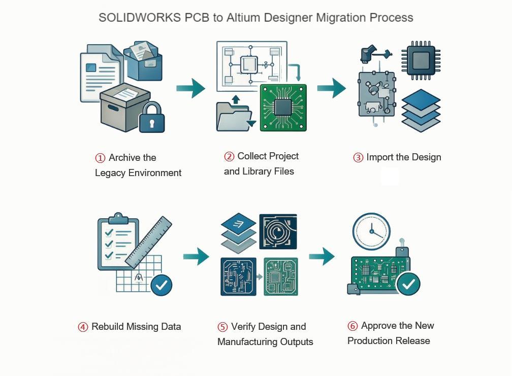
Step 1: Preserve the Original Environment
Before converting anything, archive:
- Complete project directories
- Schematic files
- PCB files
- File-based libraries
- Database-library information
- 3D component models
- Design-rule exports
- Output configurations
- Drafting templates
- Fonts and scripts
- Custom extensions
- Previously released fabrication files
- Previously released assembly files
- Original software version and service pack
- Installation records
- License records permitted by the applicable agreement
Keep at least one untouched archive. Perform the migration on a separate copy.
Step 2: Establish the Reference Revision
Identify the latest approved and manufactured revision.
Collect the production package associated with that revision, including:
- Approved Gerber or intelligent manufacturing data
- NC Drill files
- Fabrication drawing
- Assembly drawing
- BOM
- Pick-and-place data
- Approved engineering questions
- Approved deviations
- Test information, where available
This package provides a known reference for evaluating the migrated project.
Step 3: Clean the Legacy Project
If the original environment still functions, open the design before migration and resolve known warnings.
Confirm that:
- The schematic and PCB are synchronized
- Required libraries are accessible
- The correct project revision has been selected
- Obsolete drafts are separated from released files
- Missing models are identified
- Existing design-rule violations are documented
Cleaning the original project makes it easier to distinguish pre-existing issues from migration-related changes.
Step 4: Import the Project
Follow Altium’s current migration procedure for SOLIDWORKS PCB.
Perform the conversion on a copy and record:
- Original SOLIDWORKS PCB version
- Original service pack
- Altium Designer version
- Migration date
- Engineer responsible for the migration
Do not overwrite the original design files.
Step 5: Import and Review the Design Rules
Export the SOLIDWORKS PCB rules as a .rul file and import them into Altium Designer.
After import, review:
- Rule values
- Rule names
- Rule scopes
- Rule priorities
- Enabled states
- Layer assignments
- Net-class assignments
- Exceptions
Imported rules should be treated as items requiring approval, not as automatically verified data.
Step 6: Validate the Schematic
Check:
- Sheet hierarchy
- Component designators
- Net names
- Power ports
- Hidden pins
- Footprint assignments
- Unconnected pins
- Duplicate designators
- Component parameters
- Variants
- Schematic-to-PCB synchronization
Investigate warnings rather than clearing reports without review.
Step 7: Audit the PCB Structure
Verify:
- Board dimensions
- Board outline
- Cutouts
- Coordinate origin
- Layer count
- Layer order
- Copper thickness
- Dielectric thickness
- Mechanical-layer assignments
- Plated holes
- Non-plated holes
- Slots
- Blind and buried vias
- Microvias
- Copper pours
- Plane connections
- Mask openings
- Paste openings
- Text
- Component side
- Component rotation
- Keepout areas
For rigid-flex designs, also review all rigid regions, flex regions, stack transitions, coverlay definitions, stiffeners, and bend zones.
Step 8: Compare the Original and Migrated Designs
Compare measurable design data wherever possible:
- Component count
- Net count
- Unrouted connection count
- Board dimensions
- Copper layers
- Drill count
- Drill sizes
- Plated and non-plated holes
- Pad count
- Via count
- Copper geometry
- Solder-mask openings
- Paste-mask apertures
- Silkscreen
- Component coordinates
- Mechanical features
Any unexplained difference should be investigated.
Step 9: Regenerate the Manufacturing Package
Do not reuse an old manufacturing package for a modified migrated project.
Create a controlled Output Job and regenerate all required files from the migrated source.
The new package should be assigned its own revision and should not be mixed with files from the legacy release.
Step 10: Perform an Independent CAM Review
Open the newly generated outputs in an independent CAM or Gerber viewer.
Check:
- Layer alignment
- Board outline
- Copper geometry
- Drill alignment
- Drill sizes
- Slots
- Mask openings
- Paste apertures
- Silkscreen
- Polarity markings
- Component coordinates
Where possible, compare the new output with the previously approved production package.
Step 11: Request a PCB DFM Review
Before production, send the complete migrated package to the intended PCB supplier for design-for-manufacturing review.
A DFM review may identify:
- Unsupported stackup
- Insufficient annular ring
- Copper too close to the board edge
- Incorrect via structure
- Unclear slots or cutouts
- Solder-mask slivers
- Conflicting impedance information
- Missing rigid-flex details
- Incomplete fabrication notes
- Contradictory files
Step 12: Consider a Controlled First Build
For a high-value, high-speed, HDI, rigid-flex, safety-related, or mechanically constrained product, consider a prototype or controlled first-article build before authorizing normal production quantities.
The need for this step depends on the complexity of the migration, the number of design changes, historical production experience, and the product’s qualification requirements.
Common Migration Mistakes
Assuming That a Successful Import Means the Project Is Complete
A project can open without errors while still containing incorrect rules, missing models, outdated library references, or incomplete output settings.
Mixing Files from Different Revisions
Do not combine newly generated Gerber files with an old drill file, drawing, BOM, or pick-and-place file.
Every production file should come from the same approved source revision.
Treating a 3D Model as the Complete Manufacturing Definition
A STEP or Parasolid model can communicate board geometry and component placement, but it does not replace copper data, drill files, stackup information, fabrication drawings, or process specifications.
Failing to Preserve the Original Environment
Even after migration, keep a controlled archive of the original project, software information, libraries, and approved manufacturing package.
The archive may be needed to investigate an earlier revision or verify a migration difference.
Changing the Design During Migration Without Recording It
Migration and redesign should ideally be handled as separate activities.
If footprints, components, routing, stackup, or design rules must change during conversion, document those changes through the company’s engineering change process.
Skipping the Supplier’s DFM Review
Passing DRC does not guarantee manufacturability.
The CAD system checks the design against the rules entered by the designer. A PCB supplier evaluates it against actual materials, equipment, process capability, and production tolerances.
Which Platform Should You Choose?
For a New PCB Project
Between these two products, Altium Designer is the practical choice because it remains under active development.
SOLIDWORKS PCB should not be selected as the foundation for a new long-term PCB design program.
For an Existing SOLIDWORKS PCB Project
A preserved legacy environment may be used temporarily when only limited maintenance is required.
However, the company should archive the complete toolchain and prepare a migration plan before workstation failure, license problems, or operating-system changes make recovery difficult.
For Teams Using SOLIDWORKS Mechanical CAD
Altium Designer can continue working with SOLIDWORKS through MCAD CoDesigner.
If repeated bidirectional collaboration is unnecessary, a controlled STEP or Parasolid exchange process may also be sufficient.
Confirm current software compatibility before deployment.
For High-Speed, HDI, or Rigid-Flex Products
Use an actively supported ECAD platform and involve the PCB supplier early.
Software features are important, but the following factors also directly affect yield, cost, and lead time:
- Stackup feasibility
- Material availability
- Copper thickness
- Via structure
- Impedance requirements
- Registration tolerance
- Rigid-flex construction
- Special processes
For Budget-Sensitive Teams
Do not compare license prices alone.
The total cost of an ECAD platform may include:
- Software licenses
- Subscription or maintenance
- Training
- Library migration
- Design-rule conversion
- Mechanical integration
- Data management
- Version control
- Workflow development
- Technical support
- Manufacturing errors
- Future access to legacy data
Current pricing and feature entitlement should be confirmed directly with the software provider.
Final Verdict
In 2026, Altium Designer vs. SOLIDWORKS PCB is primarily a product-lifecycle and migration decision rather than a close comparison between two current ECAD platforms.
SOLIDWORKS PCB provided a useful connection between electronic and mechanical design. However, SOLIDWORKS PCB 2023 SP3 was the last supported release of both SOLIDWORKS PCB and SOLIDWORKS PCB Connector.
Existing installations may continue to support legacy products, but they should not be relied upon indefinitely without a recovery and migration plan.
Altium Designer is the more practical option for teams that want to:
- Start new PCB projects in an actively maintained environment
- Migrate related SOLIDWORKS PCB data
- Continue collaborating with SOLIDWORKS mechanical CAD
- Use current routing and design-rule workflows
- Standardize fabrication and assembly outputs
- Maintain a more sustainable engineering toolchain
The most important part of migration is not opening the old file. It is verifying what happens after the file is opened.
Every migrated project should be checked for connectivity, footprints, rules, stackup, mechanical geometry, component data, and production outputs before it is released to a PCB supplier.
Frequently Asked Questions
1. Is SOLIDWORKS PCB still supported?
No. SOLIDWORKS PCB 2023 SP3 was the last supported release of SOLIDWORKS PCB and SOLIDWORKS PCB Connector.
An existing installation may continue to operate, but it should be treated as a legacy environment. Companies that still rely on it should preserve the project files, libraries, installation information, license records, and previously approved production packages.
2. Can Altium Designer open a SOLIDWORKS PCB project?
Altium provides a documented migration workflow for SOLIDWORKS PCB projects.
Compatible schematic and library documents can be opened in Altium Designer. The .swpcbdoc board file is imported into an Altium PCB document, while design rules can be exported and imported separately through a .rul file.
The migrated project should still undergo complete electrical, mechanical, design-rule, and manufacturing-output verification.
3. Will a SOLIDWORKS PCB project migrate without any data problems?
This should not be assumed.
Although the related file formats provide a relatively direct migration route, the project may still contain differences involving:
- Design rules
- Layer assignments
- Libraries
- Footprints
- 3D models
- Polygons
- Variants
- Mechanical objects
- Output settings
A successful import proves that the software could read the data. It does not prove that the migrated board is ready for manufacturing.
4. Can Altium Designer work with SOLIDWORKS mechanical CAD?
Yes. Altium MCAD CoDesigner supports collaboration between Altium Designer and compatible SOLIDWORKS versions.
It allows electrical and mechanical engineers to exchange PCB design changes through an Altium Workspace. Teams should check the current compatibility requirements before installation because supported software combinations can change between releases.
5. Is a STEP file enough to manufacture a PCB?
No.
A STEP file is mainly used to communicate mechanical geometry. It can help verify the board outline, connector positions, component heights, and enclosure clearances.
PCB fabrication normally also requires:
- Copper-layer data
- Drill and route data
- Board outline
- Layer-stack information
- Fabrication drawing
- Material specifications
- Surface-finish requirements
- Controlled-impedance requirements
- Special process notes
PCB assembly additionally requires a BOM, pick-and-place data, assembly drawings, and fitted or not-fitted component information.
6. Which files should be regenerated after migrating to Altium Designer?
The complete manufacturing and assembly release package should be regenerated.
Depending on the project, this may include:
- Gerber or Gerber X2
- NC Drill and route files
- ODB++ or IPC-2581
- IPC-D-356 netlist
- Fabrication drawing
- Drill drawing
- Layer-stack documentation
- Assembly drawings
- BOM
- Pick-and-place data
- Paste-layer data
- Mechanical models
- Revision-controlled release notes
Do not combine files generated from the migrated project with files from an older revision.



0 Comments