




How do you use a universal PCB?
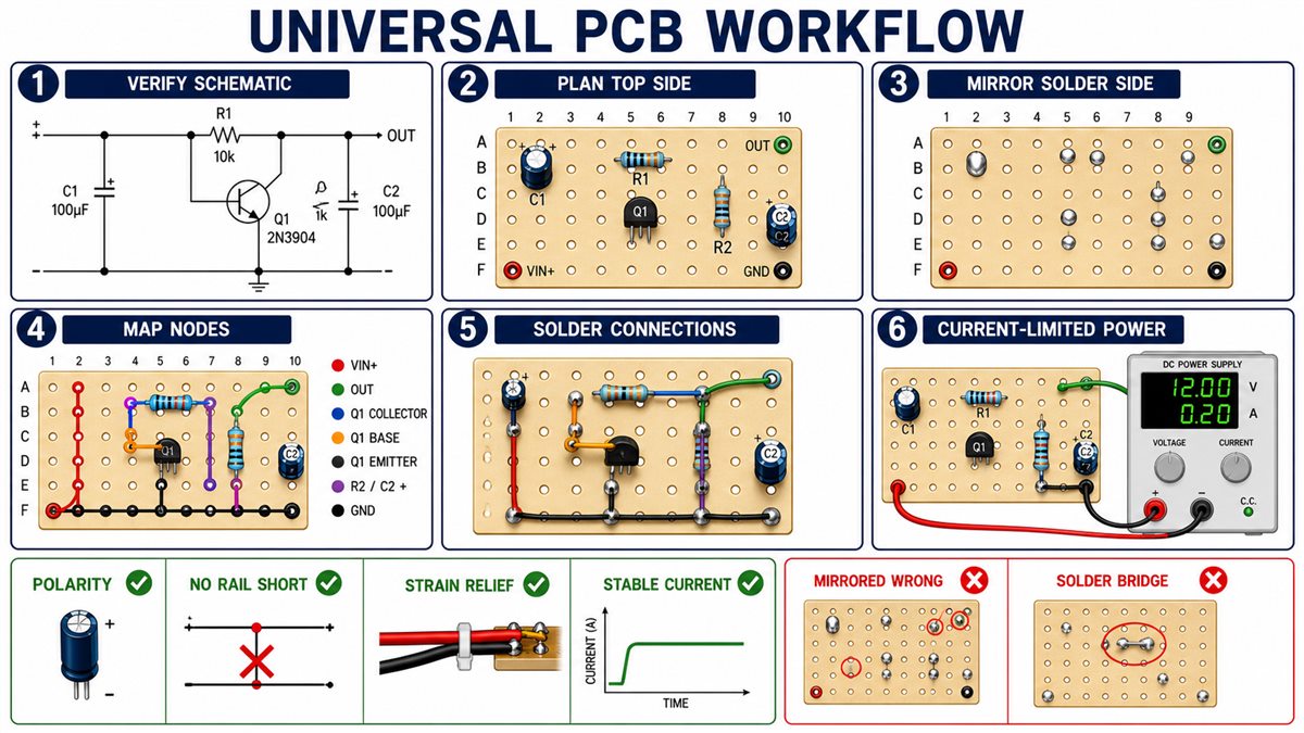
Start from a working schematic, map each electrical node onto the hole grid, place components on the top side, and make the required connections on the solder side with pad bridges, component leads or insulated wire. Inspect every node against the schematic, test for shorts, then power the board from a current-limited supply.
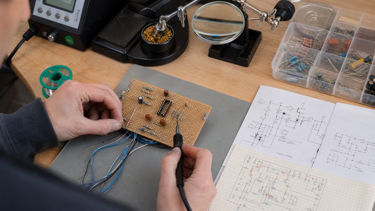
Identify the universal board type
| Board type | Copper pattern | Connection method | Best fit |
|---|---|---|---|
| Individual-pad perfboard | One isolated pad per hole | Wire or intentional solder/lead bridges | Flexible point-to-point layouts |
| Stripboard | Long copper strips | Strip cuts plus jumpers | Regular DIP circuits |
| Bus/peripheral pattern | Power rails and grouped pads | Use printed topology | Repeated modules |
| Solderless breadboard | Spring contacts, no solder | Plug-in jumpers | Temporary testing only |
Verify the circuit before transfer
Do not copy the physical breadboard blindly. Capture a clean schematic, label supply rails and net names, record component values and polarity, and confirm the prototype works over the required voltage and load. A wiring error in the breadboard should not become a permanent soldered error.
Plan the layout on paper or a grid
Draw the board from the component side and also create a mirrored solder-side view. Place connectors first, then large parts, ICs, decoupling capacitors and low-profile passives. Keep sensitive input paths away from switching nodes and make power/ground routes short enough for the circuit’s current and noise needs.
Map schematic nodes to holes
Assign each connected group a node name such as GND, +5V or MCU_RESET. Mark every component pin and every hole used by that node. Count connections at junctions. This simple net checklist is more reliable than deciding the next wire while holding a soldering iron.
Choose how to form connections
| Method | Use | Watch for |
|---|---|---|
| Bent component lead | Short local link | Mechanical stress on component |
| Tinned solid wire | Short straight bus | Uninsulated crossings |
| Insulated hookup wire | Crossovers and longer nets | Poor strain relief |
| Intentional solder bridge | Adjacent pads only | Uncontrolled blobs and hidden shorts |
Solder components in a controlled order
- Install wire links and the lowest-profile parts.
- Add sockets, resistors and small capacitors.
- Install polarized components with orientation marks visible.
- Add connectors and mechanically loaded parts with support.
- Trim leads after the joint has cooled.
- Clean residue when the flux/process requires it.
Build power and ground paths deliberately
Do not assume thin solder bridges can carry every load. Use wire gauge and path width appropriate to current, keep decoupling capacitors close to device power pins and create clear test points. For higher current, heat or safety-critical circuits, use a designed PCB rather than pushing universal board beyond a proven limit.
Inspect and test before first power
Compare each node with the schematic and mark it complete. Check diode, LED, electrolytic and IC orientation. Measure resistance between each supply rail and ground with the circuit unpowered, understanding that capacitors may make the reading change. Use continuity mode to confirm intended links, not to infer that every semiconductor path is a short.
Apply power safely
Remove socketed ICs when the design allows a rail-only test. Set the correct voltage and a conservative current limit, power the board and watch current, rail voltage, heat and smell. Stop immediately if current rises unexpectedly or a component heats. Add functional blocks one at a time rather than connecting the final load immediately.
Troubleshoot a universal PCB
| Symptom | Likely cause | Check |
|---|---|---|
| Immediate current limit | Supply short, reversed IC or solder bridge | Inspect rails and measure resistance |
| One stage is dead | Missing node or mirrored wiring error | Trace the schematic node by node |
| Intermittent operation | Cold joint, unsupported wire or connector force | Magnify joints and perform gentle stress test |
| Noisy or unstable circuit | Long ground/power loops or missing decoupling | Review layout and probe rails |
When to move to a custom PCB
Use a custom PCB when the circuit needs repeatability, fine-pitch parts, controlled grounding, high current, compliance, compact size or more than a few builds. Prepare a schematic, BOM, board outline and reviewed Gerber package.
Universal PCB checklist
- Working schematic and component values are recorded.
- Board copper pattern is understood.
- Component-side and mirrored solder-side maps exist.
- Every schematic node maps to known holes.
- Wire crossings are insulated.
- Connectors have strain relief.
- Supply-to-ground resistance is checked.
- First power uses voltage and current limiting.
Frequently asked questions
Are all holes on a universal PCB connected?
No. Perfboard pads are often isolated, while stripboard and bus boards connect defined groups. Inspect the copper side or datasheet.
How do I make traces on isolated pads?
Use component leads, tinned wire, insulated wire or short controlled bridges. Do not create long uncontrolled solder blobs.
Which side do components go on?
Components normally go on the non-copper side and are soldered on the copper side, unless the board design specifies otherwise.
Why is the solder-side layout mirrored?
Turning the board over reverses left and right. A mirrored map prevents connecting the correct pins in the wrong physical direction.
Can I carry high current on universal PCB?
Only within a verified path, wire, pad, thermal and connector limit. Move high-current or safety-related designs to a purpose-built PCB.
Can I copy a breadboard layout exactly?
Copy electrical nodes, not the breadboard’s physical rows. Universal boards have different copper connectivity.
Should I use IC sockets?
Sockets can protect heat-sensitive ICs and ease replacement, but add height and contact interfaces. Choose them by product needs.
How do I prevent wires from breaking?
Use suitable wire, avoid sharp bends, support cable exits and keep connector force out of soldered wire ends.
What files are needed for a custom PCB version?
Prepare the schematic, BOM, board outline, Gerber and drill files, assembly drawing and test requirements.
Turn the prototype into a manufacturable PCB
Send the schematic, BOM, board dimensions, interface requirements, quantity and test needs through the PCBtry contact page for PCB layout and manufacturing review.



0 Comments