




How do you make connections on a PCB board?
Choose the connection by current, signal type, mating cycles and mechanical load. Permanent component connections use soldered pads; serviceable cables use a matched board connector and crimp housing; high-current field wiring often uses rated terminals; temporary measurements use test points or clips. Finish by checking pinout, polarity, insulation, strain relief and continuity.
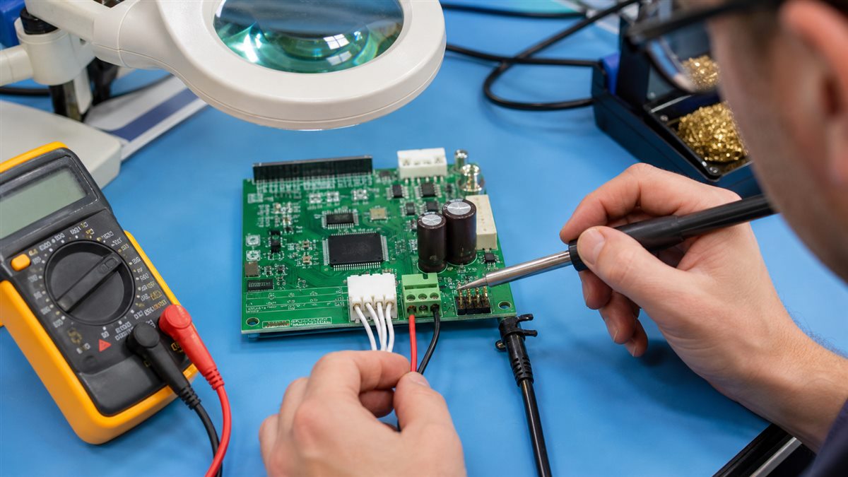
Select the connection method
| Need | Method | Key check |
|---|---|---|
| Permanent component | Soldered pad/PTH | Footprint and wetting |
| Removable cable | Header plus crimp housing | Keying, pitch and mating cycles |
| Field wiring | Screw or spring terminal | Wire range, current and torque |
| Board-to-board | Mezzanine/card-edge connector | Alignment and stack height |
| Temporary test | Test point, pogo pin or grabber | No damage or accidental short |
Define current, voltage and signal needs
Record continuous and peak current, working voltage, frequency or edge rate, environment and allowable voltage drop. A connector that fits mechanically may still be unsuitable electrically. Use the component and connector manufacturer ratings with the required derating and safety rules.
Verify footprint and pinout
Match the exact manufacturer part number to the land pattern, hole size, orientation and 3D envelope. Label pin 1, polarity and mating direction on the assembly drawing. Do not assume two visually similar headers share the same pitch or pin order.
Make a direct wire-to-pad connection
- Choose wire type and gauge for current and flexing.
- Strip only the required length without nicking strands.
- Twist and pre-tin stranded wire when the process permits.
- Clean and flux the pad, then heat wire and pad together.
- Form a smooth joint without wicking solder far into the flexible cable.
- Add strain relief so cable movement does not bend the solder joint.
Install headers and board connectors
Fixture the connector square, tack one pin and verify alignment before soldering the rest. Solder ground or mechanically significant tabs with adequate thermal capacity, but protect plastic housings from long dwell. Inspect for incomplete barrel fill, bridges and lifted pins.
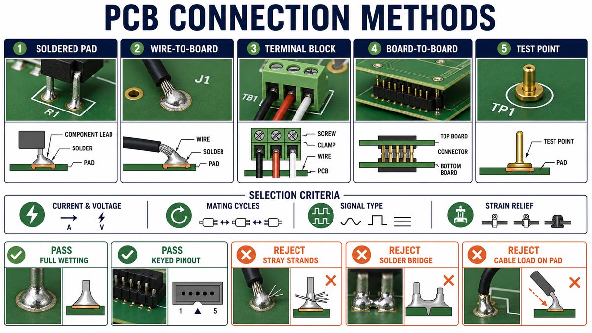
Use terminal blocks for field wiring
Confirm wire range, ferrule policy, strip length, current, voltage, temperature and tightening method. Keep the terminal’s insertion force and cable pull out of fragile PCB spans. Provide enclosure access without exposing hazardous conductors.
Connect pads on perfboard or prototype PCB
For individual pads, use component leads or correctly sized solid/insulated wire. Use short intentional solder bridges only between adjacent pads when the layout supports them. Long solder blobs are difficult to inspect and can crack or short.
Add strain relief and mechanical support
Use cable clamps, tie points, connector latches or enclosure features so vibration and pulling do not reach copper pads. Maintain bend radius and keep tie pressure away from sharp board edges. Test insertion, removal and cable pull in the real enclosure.
Inspect and test every connection
| Check | Pass | Reject |
|---|---|---|
| Pinout | Matches schematic and labels | Reversed or swapped pins |
| Solder | Wets pad and lead | Bead, crack or bridge |
| Insulation | No exposed conductor beyond need | Stray strands or damaged jacket |
| Retention | Load bypasses solder joint | Cable moves pad |
| Electrical | Correct continuity and isolation | Open, short or excess drop |
Common connection failures
Intermittent connections usually come from cold joints, unsupported wires, loose crimps, fretting contacts or connector misalignment. Overheating can lift pads or soften housings. Diagnose the mechanical condition and electrical measurement together instead of reflowing every joint blindly.
Prepare connections for production
Release exact connector part numbers and approved alternates, mating cable details, crimp contacts, pinout, wire gauge/color, strip length, torque or crimp tool, pull-test criteria and electrical test. Include these with BOM, placement and assembly files.
PCB connection checklist
- Electrical and mechanical requirements are defined.
- Exact connector and footprint match.
- Pin 1 and polarity are unambiguous.
- Wire gauge and terminal range match.
- All loaded cables have strain relief.
- Solder joints are visible and bridge-free.
- Continuity and isolation are tested unpowered.
- Mating and pull tests reflect real use.
Frequently asked questions
Can I solder a wire directly to a PCB?
Yes, for a suitable pad and wire, but add strain relief so movement does not peel the copper or fatigue the joint.
Should stranded wire be tinned before a screw terminal?
Do not assume so. Some terminals prohibit tinned conductors because solder can creep. Follow the terminal instructions and use ferrules when specified.
How do I connect two adjacent perfboard holes?
Use a short component lead or solid wire; a controlled solder bridge can work for adjacent pads but must remain inspectable.
How do I connect wires without solder?
Use a designed connector, spring terminal, screw terminal or temporary test clip. Do not improvise unreliable pressure contact for production.
What causes a PCB pad to lift?
Excess heat, force before solder melts, repeated rework and cable load can separate copper from laminate.
How do I prevent reverse connection?
Use keyed or polarized connectors, clear pin-1 markings, asymmetric footprints and an assembly test.
Can a header carry power?
Only within the exact header/contact ratings and board thermal limits. Check continuous and peak current plus temperature rise.
What is the best board-to-board connection?
It depends on pin count, current, signal integrity, spacing, alignment, vibration and service cycles; select from measured requirements.
What should a PCBA supplier receive?
Provide schematic, BOM, connector drawings, pinout, cable assembly data, assembly notes and electrical/mechanical acceptance tests.
Request a PCB connection review
Send Gerber and drill files, schematic, BOM, connector and cable details, current/voltage, mating cycles, quantity and tests through the PCBtry contact page.



0 Comments