




PCB desmear is the controlled removal of resin residue from drilled or laser-formed holes before hole metallization. Its purpose is not simply to make a hole look clean. It must expose the intended inner-layer copper, leave the dielectric surface suitable for the qualified metallization sequence, and avoid damaging the laminate or changing the hole geometry beyond the allowed process window.
The correct desmear process depends on the dielectric system, hole type, drilling method, aspect ratio, production equipment, and the evidence required by the drawing or customer specification. A chemistry recipe copied from another board is not a safe process plan.
What Is the PCB Desmear Process?
Mechanical drilling generates heat and friction as the tool cuts copper and polymer. Softened resin can be spread across the hole wall and the exposed edges of inner-layer copper. Laser drilling can leave a different mix of decomposed resin, glass reinforcement, fillers, or residue at the microvia bottom. Desmear removes this unwanted material so the following activation and copper-deposition stages can reach the surfaces they are intended to cover.
A production desmear sequence is usually treated as a set of controlled objectives rather than one universal recipe:
- Condition the hole: make the residue and dielectric surface accessible to the selected treatment.
- Remove the residue: use a qualified wet-chemical, plasma, or combined route appropriate to the material and hole.
- Remove reaction products: neutralize and rinse as required by the qualified line so residues are not carried forward.
- Verify the result: confirm hole-wall condition and inner-layer exposure using the specified inspection plan.
- Release to metallization: proceed only when the desmear evidence and line controls are acceptable.
Why Drilling Smear Threatens Hole Reliability
A plated through-hole or via is a chain of interfaces. If resin residue remains over an inner-layer connection, later activation and copper deposition may occur on the residue instead of creating the intended copper-to-copper connection. The result can be incomplete coverage, weak adhesion, an intermittent connection, or an open circuit. The defect may be obvious in a cross-section, or it may appear only after thermal and mechanical stress.
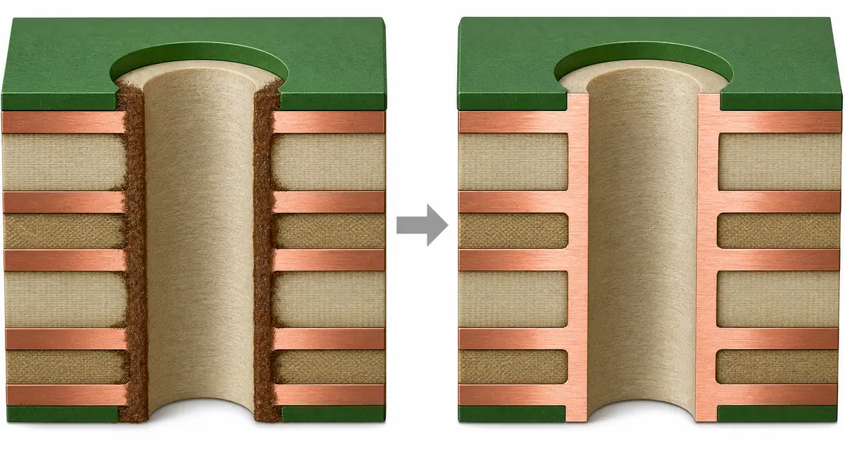
The failure chain is usually more useful than the label “poor desmear”:
drilling condition → residue location and character → treatment access → surface condition → activation/electroless copper coverage → final plated-hole evidence.
This chain also prevents a common diagnostic error. A plating void is not proof that desmear alone caused the defect. Drilling damage, inadequate rinsing, conditioner carryover, activation failure, poor solution exchange, or later plating controls may produce a similar symptom. Root-cause work should preserve evidence from adjacent stages.
Where Desmear Fits in the PCB Manufacturing Flow
For a mechanically drilled multilayer board, desmear follows drilling and hole cleaning and precedes activation and electroless copper. For HDI structures, the sequence depends on the buildup cycle and microvia formation method. Review the full PCB drilling process because drill parameters, tool condition, stack setup, and heat removal influence the residue that desmear must remove. When the design uses laser-formed vias, compare the constraints in laser drilling versus mechanical drilling.
| Stage | Question to answer | Evidence or hold point |
|---|---|---|
| Incoming construction review | What resin, reinforcement, filler, copper treatment, and hole types are present? | Approved material set, stackup, drawing, and route |
| Drilling or laser formation | What residue and damage mechanism can this operation create? | Qualified tool/laser setup and monitored process |
| Desmear | Can the chosen route reach the hole surfaces without unacceptable material attack? | Qualified loading, equipment, chemistry/plasma controls, and coupons |
| Rinse/neutralization | Were reaction products removed without harmful carryover? | Line controls defined by the qualified process |
| Activation and electroless copper | Are prepared surfaces continuously covered? | Coverage and process-control evidence |
| Product verification | Does the plated interconnect meet the applicable acceptance criteria? | Microsection and required electrical/reliability evidence |
Chemical Permanganate vs Plasma Desmear
Wet chemical and plasma desmear can both be capable processes, but they solve the access and material-removal problem differently. Selection must be based on the actual construction and a qualified production window.
| Decision factor | Permanganate-based wet process | Plasma process |
|---|---|---|
| Basic mechanism | Conditioning and oxidative removal in a controlled chemical sequence | Reactive gas species remove or modify polymer in a controlled chamber cycle |
| Typical strength | Established high-volume processing for compatible epoxy systems | Dry treatment with recipe flexibility for selected materials and difficult residues |
| Main constraint | Chemistry compatibility, solution exchange, rinsing, bath control, and waste treatment | Chamber loading, gas exposure, shadowing/uniformity, equipment capacity, and recipe control |
| Geometry concern | Wet-out and replenishment inside small or deep holes | Uniform exposure throughout the load and within the hole geometry |
| Material concern | Resin systems do not respond identically to conditioning and oxidation | Gas chemistry and energy must be qualified for the dielectric and copper interfaces |
| Verification focus | Bath/line controls plus hole-wall and downstream coverage evidence | Recipe, chamber/loading and process-monitor evidence plus hole-wall and downstream coverage |
A combined route may be justified for a difficult construction, but “more treatment” is not automatically safer. Excessive attack can change resin recession, expose or disturb reinforcement, alter surface topography, or create downstream residues. The process objective is adequate, uniform preparation—not maximum material removal.
How to Select a Desmear Route
Start with the board construction, not the name of a machine or chemistry. High-aspect-ratio holes can make solution exchange and uniform treatment harder; review the geometric issues described in high-aspect-ratio PCB manufacturing. HDI buildup and microvia structures create a different access problem, covered in our guide to HDI PCB construction.
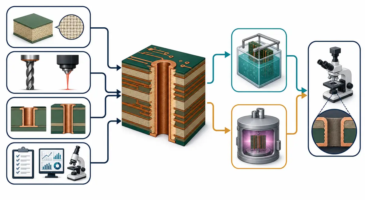
| Input | Why it changes the decision | What to confirm |
|---|---|---|
| Dielectric family and exact laminate | Epoxy, highly filled resin, polyimide, and fluoropolymer systems can respond differently | Material supplier guidance and fabricator qualification for the exact construction |
| Mechanical hole or laser microvia | The residue mechanism, location, and access path differ | Cross-sections or coupons representing the real formation process |
| Finished hole size and aspect ratio | Small/deep features increase uniformity and exchange challenges | Capability for the worst-case hole, panel position, and load |
| Required desmear or etchback | Residue removal and controlled resin recession are not interchangeable requirements | Drawing language, acceptance criteria, and measurement method |
| Downstream metallization | Surface preparation must be compatible with activation and copper deposition | A qualified end-to-end route, not isolated desmear capability |
| Production volume and controls | Throughput, loading, replenishment, monitoring, maintenance, and waste constraints differ | Control plan, reaction plan, and traceability |
Stop and escalate when the fabricator cannot show qualification for the specified material/hole combination, when the drawing uses ambiguous desmear/etchback language, when a laminate change is proposed after qualification, or when product evidence conflicts with process-monitor data.
Critical Process Controls and Failure Modes
Under-treatment
Residual resin can remain over inner-layer copper or on the hole wall. Likely contributors include excessive drilling smear, inadequate conditioning, insufficient treatment, poor access in challenging geometry, depleted or out-of-control chemistry, nonuniform plasma exposure, or an unqualified material change. The corrective action is not simply to extend time: first verify the residue mechanism, material, loading, equipment status, and cross-section evidence.
Over-treatment
Excessive resin removal or surface modification can change the intended interface. Depending on the construction, concerns may include too much recession, reinforcement exposure, nonuniform texture, or weakened material. Compare measured product evidence with the allowed drawing and qualified-process limits before changing the route.
Poor uniformity
A passing monitor at one position does not prove every hole in every panel received equivalent treatment. Panel spacing, rack or chamber loading, hole geometry, wetting, flow, and plasma exposure can create positional differences. Qualification coupons should represent credible worst cases, and production monitoring should detect drift in the factors known to control uniformity.
Carryover or incomplete cleanup
Reaction products or process residues carried into activation can compromise later coverage even if resin was removed. Rinse and neutralization stages therefore need their own controls. Do not judge desmear only by how much material was removed.
Wrong root cause
When a plated-hole defect appears, keep evidence from drilling, desmear, activation, electroless copper, and electrolytic plating. A disciplined review avoids adjusting desmear until the true cause is known.
How Manufacturers Verify Desmear Results
Verification has two layers. Process monitoring shows that equipment and chemistry operated within the qualified window. Product acceptance shows that the board or representative coupon meets the specified result. One cannot automatically replace the other.
- Microsection/cross-section: inspect representative holes for residue, inner-layer exposure, hole-wall condition, and the completed plated interface.
- Coverage evidence: confirm the activation and electroless copper sequence created continuous coverage where required.
- Process-control records: review the relevant chemistry, equipment, loading, time/sequence, maintenance, and reaction-plan records defined by the qualified route.
- Electrical and reliability evidence: use the tests required by the drawing, customer, product class, and applicable specification. Desmear appearance alone does not prove long-term interconnect reliability.
- Traceability: link material lot, drilling/laser route, desmear batch or cycle, coupons, and acceptance records.
Acceptance language must cite the applicable document and revision. IPC standards provide industry frameworks, but the purchase drawing and customer requirements determine what applies to a specific order. Do not invent a universal resin-recession number or assume a photomicrograph is acceptable without its scale, location, preparation method, and acceptance reference.
A Source-Bounded Process Lesson
A 1996 technical report from Sandia National Laboratories and collaborators examined process uniformity for plasma etchback and desmear in printed wiring board manufacturing. The report states that insufficient plasma treatment can leave inadequate polymer removal at internal-layer copper, leading to circuit discontinuity during plating. It also emphasizes board placement, pretreatment, treatment conditions, post-plasma testing, and continuous process monitoring, and discusses optical emission spectroscopy as an in-situ monitoring approach.
Practical lesson: a plasma recipe name or nominal cycle is not proof of uniform treatment. Loading, pretreatment, monitoring, and post-process verification belong to the same control plan. This historical report does not establish a modern universal recipe or acceptance limit; it supports the durable engineering principle that desmear must be controlled and verified as a production process.
Desmear Supplier Brief and Pre-Plating Checklist
Information to send the fabricator
- Approved laminate manufacturer, grade, thicknesses, resin/reinforcement details, and permitted alternatives
- Stackup, copper weights, finished board thickness, and inner-layer connection structure
- Mechanical-hole and laser-microvia populations, minimum diameters, depths, and aspect ratios
- Drawing requirements for desmear, etchback, plated holes, coupons, and acceptance
- Product class, applicable specifications/revisions, reliability tests, and any customer-specific controls
Questions to ask before release
- Is the exact dielectric/hole combination covered by an approved desmear and metallization qualification?
- Which route is proposed, and what construction-specific evidence supports it?
- How are worst-case hole geometry, panel position, and production loading represented?
- How are under-treatment, over-treatment, poor uniformity, and carryover detected?
- Which microsection, coverage, electrical, and reliability records will be delivered?
- What changes require requalification or customer approval?
Need a manufacturability review? Send PCBtry your stackup, laminate grade, hole table, aspect ratios, drawing notes, and required acceptance standard. We can review whether the information is sufficient for a fabricator to define and verify an appropriate desmear-to-metallization route. Final process parameters remain the responsibility of the qualified manufacturer.
Frequently Asked Questions About PCB Desmear
1. What is smear in PCB drilling?
Smear is resinous material displaced or redeposited on a drilled hole wall, especially across exposed inner-layer copper. Its amount and character depend on the material and drilling conditions.
2. Why is desmear performed before copper plating?
Desmear exposes the intended surfaces so activation and copper deposition can form the specified interconnect. Plating over residue can create incomplete or unreliable interfaces.
3. Is desmear the same as etchback?
No. Desmear removes drilling residue. Etchback deliberately recesses dielectric around inner-layer copper. A qualified process may accomplish both, but the requirements must be stated and verified separately.
4. What are the main PCB desmear methods?
Permanganate-based wet chemical processing and plasma processing are common routes. Some constructions use a combined or specialized sequence. The choice must be qualified for the material, hole, and downstream metallization.
5. Is plasma desmear always better than chemical desmear?
No. Plasma offers useful dry-process and material-specific capabilities, while wet chemistry can be an established high-volume route for compatible systems. Uniformity, capacity, material response, controls, cost, and evidence determine the better choice.
6. Does every PCB need desmear?
Not every board has the same need or route. The fabricator determines hole preparation from the construction, drilling method, metallization sequence, drawing, and qualified process. Multilayer plated holes commonly require controlled residue removal.
7. How does desmear differ for laser microvias?
Laser formation can leave residue at the via bottom and sidewall that differs from mechanical drilling smear. Via geometry, dielectric composition, laser settings, and access to the target pad influence the qualified cleanup process.
8. Can too much desmear damage a PCB?
Excessive or incompatible treatment can modify the dielectric more than intended, create nonuniform recession, expose reinforcement, or affect later interfaces. More removal is not automatically better.
9. How is desmear quality inspected?
Manufacturers combine qualified process controls with representative microsections and downstream metallization evidence. Electrical or reliability tests are added when required by the drawing, product class, or customer specification.
10. What causes an incomplete desmear result?
Possible causes include excessive drilling residue, inadequate conditioning, an out-of-control chemistry or plasma cycle, poor hole access, nonuniform loading, incompatible materials, or process drift. Evidence should be reviewed before adjusting treatment.
11. Does high aspect ratio make desmear harder?
It can. Small, deep holes make wetting, solution exchange, reaction-product removal, and uniform exposure more difficult. Qualification should represent the worst-case geometry and production position.
12. What should a PCB drawing say about desmear?
The drawing should identify applicable specifications and revisions, any required etchback or prohibited condition, plated-hole acceptance, coupon/test requirements, and customer-specific controls. Avoid ambiguous copied notes.
13. Can a plating void prove that desmear failed?
No. A void may originate in drilling, desmear, rinsing, activation, electroless copper, or later plating. Root-cause analysis should preserve and compare evidence from the entire sequence.
14. What data should a buyer request from the PCB manufacturer?
Request material and process qualification for the construction, traceable process-control records, representative microsection results, applicable acceptance evidence, and the change-control conditions that would trigger requalification.
Technical boundary: This guide explains manufacturing decisions and verification logic. It is not a bath recipe, equipment recipe, or substitute for chemical supplier instructions, facility safety controls, environmental requirements, an approved fabrication specification, or a qualified process.



0 Comments