




The LED PCB lamination process bonds the circuit copper, electrically insulating thermal dielectric, and metal base into a stable heat-spreading structure. For a common single-layer aluminum LED PCB, this is structural insulated-metal-substrate (IMS) lamination—not photosensitive dry-film lamination. The manufacturing objective is to create a continuous, controlled dielectric interface that transfers heat while maintaining electrical isolation and adhesion.
There is no universal press temperature, pressure, vacuum time, cure time, or dielectric thickness for every LED PCB. The material supplier’s process guidance, the fabricator’s qualified equipment window, the board drawing, and the required product evidence must agree before production.
What Does LED PCB Lamination Mean?
“Lamination” can describe several different PCB operations. Clarifying the intended operation prevents an RFQ from reaching the wrong process line:
- IMS or metal-core structural lamination: bonds copper foil and a thermally conductive insulating dielectric to an aluminum or copper base. This is the primary subject of this guide.
- Conventional multilayer lamination: bonds patterned cores and prepreg into a multilayer FR-4 or hybrid board. It may be relevant to complex LED controls but is not the standard three-layer MCPCB route.
- Photoresist dry-film lamination: applies a photosensitive film before imaging and etching. It occurs later in circuit formation and does not create the structural thermal stack.
- Assembly thermal-interface bonding: joins a finished board to a heatsink or chassis. That interface affects system temperature but is not PCB laminate fabrication.
How an LED Metal-Core PCB Stack Is Built
A basic single-layer LED metal-core PCB has three functional layers:
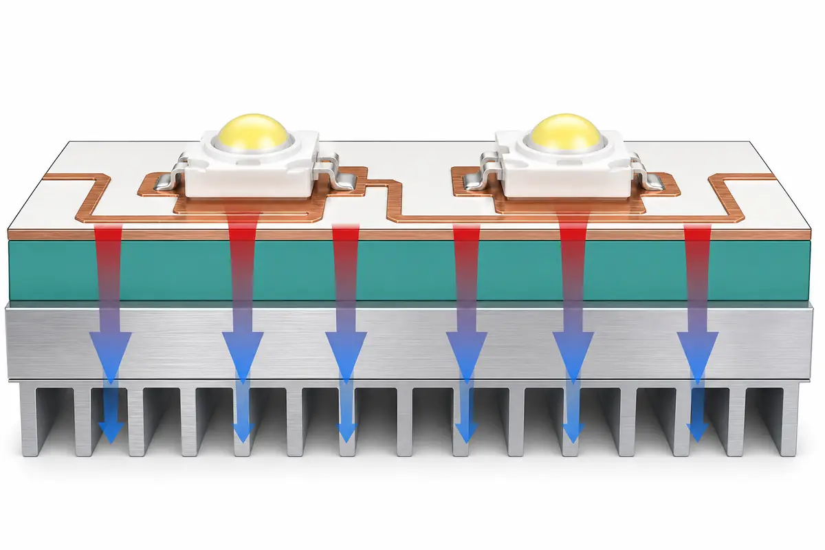
- Circuit copper: carries current and spreads heat laterally from LED pads. Its foil type, thickness, surface treatment, copper distribution, and etched geometry influence bonding and dimensional behavior.
- Thermally conductive dielectric: electrically isolates copper from the metal base while conducting heat through its thickness. Composition, thickness, cured state, void content, breakdown behavior, adhesion, and thermal test method all matter.
- Metal base: provides stiffness and spreads heat toward the luminaire housing or heatsink. Aluminum is common, but copper and other qualified constructions are used when their performance and cost are justified.
The complete thermal path continues beyond the laminate: LED junction → package thermal path → solder joint → copper pad → dielectric → metal base → board-to-housing interface → heatsink or chassis → ambient. Our guide to aluminum PCB thermal management for LED lighting explains why the dielectric and external interfaces can dominate the result even when the metal base conducts heat well.
Not every LED application needs a metal-core board. Start with thermal, electrical, routing, mechanical, cost, and reliability requirements rather than assuming “LED” means “aluminum PCB.”
The LED PCB Lamination Process Step by Step
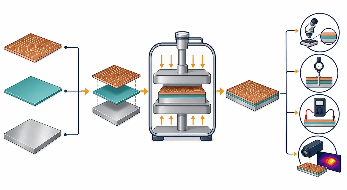
1. Freeze the construction and process route
The fabricator confirms the approved dielectric system, copper foil, metal base, finished dimensions, surface condition, and acceptance requirements. It must also establish whether production begins with a material supplier’s pre-bonded IMS laminate or whether the fabricator is qualified to bond a custom construction. A material trade name alone is insufficient when thickness, foil, base, cure state, or test method can vary.
2. Inspect and condition incoming materials
Identify and handle copper, dielectric, and metal base under the supplier and qualified-process rules. Contamination, oxidation, moisture, expired shelf life, or substitution can change flow, adhesion, and isolation. Keep lot and condition traceable.
3. Prepare the bonding surfaces
Use the qualified cleaning and preparation route to remove oil, particles, loose oxide, water, and incompatible residues. Surface treatment must match the material system; “rougher is always better” is not a valid rule.
4. Cut and lay up the stack
Cut and align materials while protecting bonding interfaces. Tooling, release materials, caul plates, cushions, separators, and panel spacing belong to the qualified package because they affect heat, pressure, surface condition, and thickness.
5. Remove trapped air and apply the qualified press cycle
A qualified air-removal method reduces trapped air. Heat changes resin viscosity and cure; pressure promotes contact and flow. Timing, heating rate, platen uniformity, vacuum, and load interact, so matching nominal peak settings alone does not reproduce a process.
6. Complete cure and cool under control
The cycle must deliver the required cure throughout the load. Cooling and pressure release affect residual stress and flatness because copper, filled dielectric, metal base, and tooling expand differently.
7. Release, inspect, and continue circuit fabrication
After release, inspect thickness, flatness, blistering, edge separation, and specified conditions. Later circuit fabrication and heat can reveal a weak interface, so traceability continues beyond the press.
Which Material and Construction Inputs Control the Result?
The dielectric is not selected by conductivity alone. Thickness, isolation, tolerance, adhesion, cure, voids, test method, and reliability matter. A simple layer model relates thermal resistance to thickness, conductivity, and area, but a real LED assembly also includes spreading, copper geometry, package, solder, mounting interface, heatsink, and convection.
Copper thickness, treatment, and distribution affect current, spreading, etching, bonding, flow, and stress. Base alloy, temper, thickness, flatness, surface condition, and cleanliness affect adhesion and mechanics. Long LED bars, asymmetric copper, slots, holes, later soldering, and mounting can change flatness or load the interface. Qualify the full construction rather than substituting one nominal property.
How to Select the Right Lamination Route
| Decision input | Why it matters | Required supplier answer |
|---|---|---|
| LED heat load and allowed temperatures | Defines the thermal path the board must support | Board/system thermal model or test plan with stated boundaries |
| Operating voltage and isolation requirement | Constrains dielectric construction and validation | Applicable standard, test voltage/method, spacing and acceptance |
| Routing complexity | Determines whether single-layer IMS is sufficient | Recommended IMS, multilayer metal-backed, FR-4, ceramic or alternative architecture |
| Dielectric family and thickness | Balances heat transfer, isolation, adhesion and processing | Exact approved material construction and test-method-compatible data |
| Copper and metal base | Affects spreading, current, mass, flatness, etching and cost | Foil/base alloy, thickness, treatment and substitution controls |
| Pre-bonded versus custom lamination | Changes who owns material bonding qualification | Source of bonded laminate, scope of fabricator qualification and lot traceability |
| Board size and copper balance | Changes thickness and warpage risk | Panelization, tooling, copper balance and flatness plan |
| Evidence required | Prevents acceptance based on a marketing conductivity number | Process records plus specified interface, adhesion, isolation and thermal results |
For general material terminology, use our guide to PCB substrates, cores and dielectric materials. If the design is genuinely multilayer rather than a single-layer IMS board, the sequence in multilayer PCB stackup and lamination is the more relevant starting point.
Stop and escalate when the exact material construction is not named, a supplier proposes a dielectric or base substitution without comparison and approval, isolation and thermal values use unclear test methods, the fabricator cannot identify who qualified the bonding operation, or production evidence conflicts with board-level inspection.
Critical Lamination Defects and Root Causes
| Observed condition | Possible contributors | Evidence to preserve |
|---|---|---|
| Voids or incomplete contact | Trapped air, contamination, inadequate air removal, incompatible flow, poor surface condition or nonuniform pressure/heat | Cross-section or imaging, position map, material lot, surface-prep and press records |
| Blister or delamination | Weak interface, moisture, contamination, inadequate cure, thermal stress or later-process exposure | Failure interface, thermal history, moisture/storage, adhesion and material identification |
| Excessive or inadequate dielectric flow | Wrong material/cure state, temperature-pressure timing, load, thickness or copper topography | Finished dielectric profile, edge condition, press trace and layup record |
| Thickness nonuniformity | Tooling/pressure variation, copper imbalance, material variation, panel geometry or flow | Panel thickness map, copper distribution, load position and tooling setup |
| Warpage or bow/twist | CTE mismatch, asymmetric construction, uneven copper, thermal gradients or uncontrolled cooling/release | Before/after flatness, panel orientation, cycle and copper balance |
| Isolation failure | Thin spot, void, contamination, damage, incorrect dielectric or later fabrication defect | Failure location, dielectric thickness/interface section, test setup and lot records |
| Unexpected LED hot spot | Laminate void or thickness variation, but also LED package, solder, copper layout, mounting interface or heatsink | Thermal map correlated with cross-section, assembly interface and electrical load |
A hot spot is not proof of bad lamination, and a peel failure does not identify the failed interface. Locate the separation, preserve samples, compare panel position and lot history, and review the full heat path before changing the press cycle.
How Manufacturers Verify a Laminated LED PCB
Process monitoring shows that a load followed the qualified route. Product acceptance shows that boards or coupons meet the specified result. Neither automatically replaces the other.
- Traceability: approved material, lot/batch, shelf life, storage, surface preparation, press load and operator/equipment records.
- Cycle evidence: the parameters defined by the qualified process, recorded in a way that represents the actual load rather than a typed nominal recipe.
- Thickness and flatness: specified sampling across credible worst-case panel positions and board geometry.
- Interface evidence: visual inspection, cross-section or another approved method to evaluate voids, layers, dielectric profile and failure location.
- Adhesion evidence: a specified test method and conditioned state; do not compare peel values from different constructions or methods as if they were interchangeable.
- Electrical isolation: dielectric withstand, insulation resistance or other tests defined by the product and applicable safety requirements.
- Thermal evidence: material characterization, coupon tests, board tests or system thermal validation with clear boundaries, sensors, loads and interfaces.
- Reliability evidence: thermal cycling/shock, reflow exposure, humidity, power cycling or mechanical evaluation when required by the application and specification.
Confirm the applicable IPC, UL, IEC, customer or product requirements and their revisions for the actual order. This article deliberately does not invent a universal breakdown voltage, peel strength, void limit, press setting or thermal-cycling requirement.
A Source-Bounded MCPCB Lamination Lesson
A published study titled “Development of Epoxy/BN Composites with High Thermal Conductivity for Metal-Core Printed Circuit Board (MCPCB)” describes preparing thermally conductive epoxy composites for MCPCB by varnish coating and hot pressing. The abstract reports that filler type and combination changed the measured thermal behavior and explicitly states that reducing voids, controlling filler shape, and surface modification were important for achieving high conductivity.
Problem: an MCPCB dielectric must combine heat transfer with electrical insulation, but adding nominally conductive filler does not guarantee the best composite result. Treatment and action: the researchers compared different filler combinations in epoxy and used a coating/hot-press preparation route while considering void reduction and filler/surface characteristics. Reported result: some secondary BN filler combinations outperformed the alumina-only comparison, while one hexagonal-BN-filled composite did not, despite BN’s high intrinsic conductivity.
Factory lesson: headline filler conductivity is not enough. Lamination quality, void control, filler morphology, surface treatment, dielectric formulation and the validated test method interact. This laboratory study does not supply a universal LED PCB press recipe, field-life result, or qualified production material; it supports the narrower decision principle that composite and process behavior must be measured in the actual construction.
LED PCB Lamination RFQ and Release Checklist
Define before quoting
- LED part numbers, quantity and power map, drive conditions, ambient range and cooling arrangement
- Maximum allowed LED junction, board reference-point and housing temperatures with measurement/model boundaries
- Exact layer stack, copper thickness, dielectric requirement, base metal/alloy/thickness and permitted alternatives
- Board outline, long-strip geometry, panelization, holes/slots, copper balance and flatness requirement
- Operating voltage, electrical isolation, creepage/clearance and applicable safety/product standards
- Surface finish, soldering profile, mounting method, thermal-interface material and heatsink/chassis condition
Ask the manufacturer
- Is the IMS supplied pre-bonded, or does the fabricator perform the copper-dielectric-metal lamination?
- Who owns and maintains qualification for the exact material, foil, base and thickness combination?
- How are metal/copper surface preparation, interface cleanliness, material storage and shelf life controlled?
- How does the press control actual load temperature, pressure, air removal, cure and cooling?
- How are worst-case panel positions and long/asymmetric LED boards represented?
- What evidence covers dielectric thickness, voids/interface, adhesion, flatness, isolation and thermal performance?
- Which material, supplier, base alloy, thickness, tooling, cycle or site changes trigger approval or requalification?
Need an LED PCB manufacturability review? Send PCBtry the stackup, LED power map, voltage/isolation requirements, board outline, copper data, material preferences, heatsink interface, operating environment and validation plan. We can identify missing RFQ inputs and review whether the proposed evidence covers the laminate and system risks. Final material selection and press parameters remain with the qualified material supplier and manufacturer.
FAQ About LED PCB Lamination
1. What is the LED PCB lamination process?
For a typical metal-core LED PCB, it is the qualified bonding of circuit copper, a thermally conductive electrical dielectric, and a metal base using controlled surface preparation, layup, air removal, heat, pressure, cure and cooling.
2. Is LED PCB lamination the same as dry-film lamination?
No. Structural lamination creates the bonded substrate. Dry-film lamination applies photosensitive resist for later circuit imaging and etching.
3. Are all LED PCBs aluminum-core boards?
No. The appropriate construction can be aluminum or copper IMS, FR-4, high-Tg multilayer, ceramic, flexible, or another architecture depending on heat, routing, isolation, mechanics, cost and reliability.
4. What layers are in a basic aluminum LED PCB?
A common single-layer construction contains circuit copper, a thermally conductive insulating dielectric, and an aluminum base. Solder mask, surface finish and assembly materials are added but are not the three structural laminate layers.
5. Why is the dielectric layer important?
It must transfer heat while electrically isolating copper from the metal base and maintaining adhesion and reliability. Thickness, composition, cure, voids and test method all affect performance.
6. Does higher dielectric thermal conductivity always make a better LED PCB?
No. Actual performance also depends on dielectric thickness, voids, copper spreading, LED package, solder, metal base, mounting interface, heatsink and test conditions. Isolation and reliability must not be sacrificed.
7. What causes voids during LED PCB lamination?
Possible contributors include trapped air, contamination, poor surface condition, inadequate air removal, incompatible material flow, nonuniform heat/pressure, or a cycle outside the qualified material window.
8. What causes an aluminum PCB to delaminate?
Potential causes include interface contamination, moisture, incorrect material or surface treatment, inadequate cure, thermal stress, incompatible later processing or mechanical loading. The actual failure interface must be identified before correction.
9. Can press temperature and pressure be copied from another MCPCB?
No. The correct cycle depends on the exact dielectric, copper, metal base, tooling, load, equipment and supplier qualification. Use the approved material and process documentation.
10. How is LED PCB lamination quality checked?
Checks may include traceable process records, thickness/flatness, interface inspection or cross-section, adhesion, electrical isolation and thermal or reliability testing as required by the drawing and application.
11. Can a thermal-camera hot spot prove a laminate void?
No. The hot spot could originate in the LED package, solder, copper layout, laminate, board-to-heatsink interface, heatsink or airflow. Correlate thermal data with structural and process evidence.
12. Is a pre-bonded IMS laminate safer than custom in-house lamination?
Not automatically. Pre-bonded material can simplify ownership of the bonded laminate, while custom bonding can enable special constructions. In either case, qualification, incoming controls, fabrication compatibility and change control must be clear.
13. What should be included in an LED PCB lamination drawing?
Define the stack, exact or approved material family, copper and base thickness, dielectric/isolation requirements, finished dimensions and flatness, applicable standards, tests, coupons and substitution/change controls.
14. What evidence should a buyer request?
Request exact-construction qualification, lot traceability, surface-preparation and press-cycle controls, representative interface/thickness results, specified adhesion and isolation tests, relevant thermal evidence and requalification triggers.
Technical boundary: This article is a manufacturing decision and verification guide, not a press recipe, safety procedure, material datasheet, qualification certificate or substitute for supplier processing instructions and applicable product standards.



0 Comments