




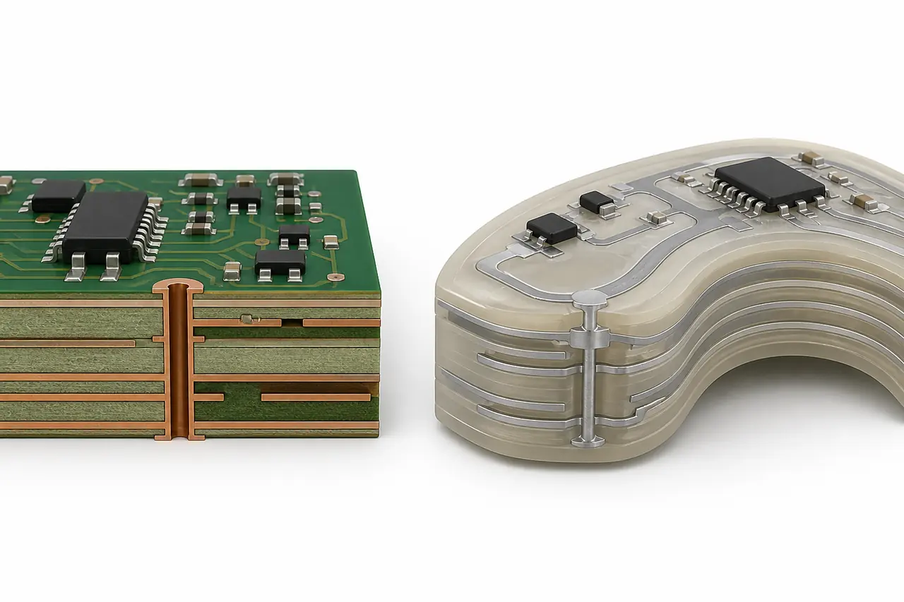
A 3D printed circuit board is an electronic interconnect structure made partly or largely by additive manufacturing. Instead of patterning copper on a flat laminate only, the process deposits dielectric and conductive materials where they are needed. The result may be a multilayer planar board, a circuit printed on a curved carrier, or a hybrid structure with conductors embedded inside a printed polymer.
The name is broader than it sounds. Some systems co-print dielectric and conductive layers; others print a plastic carrier first and add conductive ink, plating, or components later. These routes can shorten design iterations and put circuitry on shapes that a conventional rigid PCB cannot follow. They do not automatically match the conductivity, temperature capability, fine geometry, reliability evidence, or production ecosystem of copper-clad FR-4.
The Short Answer: What Counts as a 3D Printed Circuit Board?
Engineers use “3D printed PCB” for several related constructions. Before comparing quotations or design rules, identify which one a supplier means:
| Construction | What is additive? | Typical description | Important boundary |
|---|---|---|---|
| Co-printed multilayer electronics | Dielectric and conductive layers | Alternating insulating and functional inks build a circuit layer by layer | Components are usually placed, not printed as silicon devices |
| Conformal direct-write circuit | Conductive and sometimes dielectric material | Ink is deposited on a curved or three-dimensional carrier | The carrier may be molded, machined, or printed separately |
| Printed substrate plus metallization | The carrier, channels, or masks | A polymer body is printed, then traces are plated or filled | This is a hybrid additive and metallization process |
| Conductive-filament circuit | Insulating and conductive thermoplastics | Material extrusion forms simple paths and structures | Filled polymers normally have much higher resistance than bulk copper |
Laser direct structuring on a molded interconnect device is often discussed beside these methods, but molding and laser activation are not the same as fully 3D printing a board. Likewise, a conventional PCB mounted inside a 3D-printed enclosure is not a 3D printed PCB.
How a 3D Printed Circuit Board Is Made
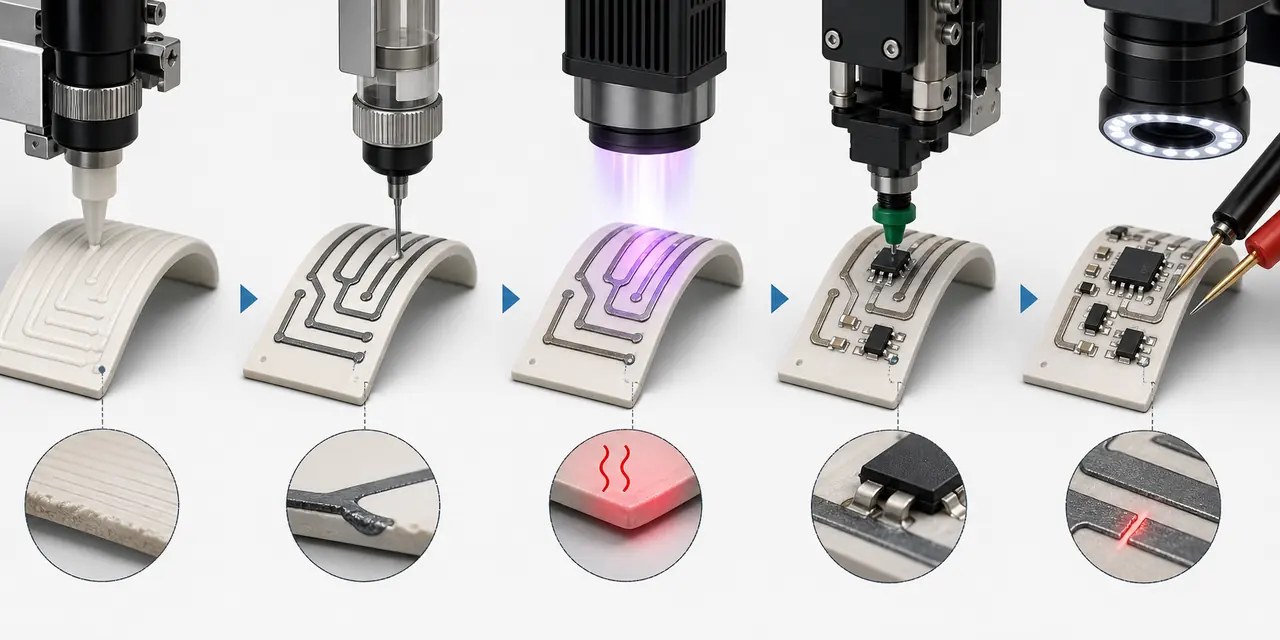
The exact equipment varies, but a credible process has more stages than “send CAD to a printer.” Each material interface must survive deposition, post-processing, assembly, and use.
- Define the electrical and mechanical envelope. Record voltage, current, frequency, impedance needs, line and spacing targets, bend or shape requirements, operating temperature, environment, volume, and qualification level.
- Choose the construction. Decide whether the circuit needs a printed multilayer body, traces on a curved carrier, embedded channels, or a conventional board connected to printed features.
- Print or prepare the dielectric. The substrate must provide adequate insulation, dimensional stability, surface quality, and adhesion. Layer ridges or pores can interrupt thin conductors.
- Deposit the conductor. Inkjet, aerosol jet, dispensing, direct ink writing, extrusion, or selective metallization creates traces and pads. The toolpath and wet material behavior both affect final geometry.
- Cure, sinter, or plate. Printed metal particles need a post-process to create a useful conductive network. The temperature and energy must be compatible with the dielectric below.
- Build interlayers and vertical connections. Dielectric coverage, registration, via filling, and isolation between conductors determine whether a multilayer structure is electrically sound.
- Attach components and inspect. Low-temperature solder, conductive adhesive, or another interconnect may be needed. Visual inspection alone cannot prove continuity, isolation, adhesion, or environmental reliability.
Six Technology Routes and Their Tradeoffs
| Route | Best-known strength | Material form | Frequent constraint |
|---|---|---|---|
| Material extrusion (FFF/FDM) | Accessible shaped substrates and embedded channels | Thermoplastic dielectric; conductive composite filament | Coarse features, anisotropy, surface roughness, and high conductor resistance |
| Direct ink writing | Wide ink-viscosity range and thicker deposited features | Pastes, particle-filled inks, conductive adhesives | Nozzle size, rheology, drying shrinkage, and path continuity |
| Inkjet printing | Digital, noncontact patterned layers | Low-viscosity conductive and dielectric inks | Drop spreading, nozzle reliability, layer registration, and cure compatibility |
| Aerosol jet printing | Fine, conformal deposition over non-planar surfaces | Aerosolized functional inks | Overspray, focus control, ink formulation, equipment, and process tuning |
| Vat printing plus metallization | Complex dielectric bodies with channels or selected surfaces | Photopolymer plus electroless/electrolytic metal | Surface preparation, plating adhesion, access, and chemical compatibility |
| Multi-material inkjet/additive system | Alternating dielectric and conductor layers in one digital build | Matched proprietary functional materials | Material choice, capital cost, throughput, assembly window, and qualification |
No route owns every advantage. Aerosol jet may be attractive for a fine conformal trace, while dispensing can build a thicker conductor. Extrusion can create a useful carrier or channel but does not make a carbon-filled filament behave like electrodeposited copper. A hybrid solution often wins: print the geometry that needs additive freedom and retain conventional copper or components where electrical performance matters most.
Conductors, Dielectrics and Component-Attachment Materials
Conductive materials
Silver nanoparticle or flake inks are common because they can provide useful conductivity after curing and are available in formulations for several printing methods. Copper inks can reduce material cost and offer attractive electrical potential, but oxidation and sintering conditions complicate processing. Carbon, graphene, carbon nanotube, and conductive-polymer systems are useful for sensors, resistive elements, flexible functions, or low-current paths; they should not be assumed to replace copper power traces.
Conductivity is not a material-name property alone. Particle loading, binder, porosity, deposited thickness, cure profile, substrate roughness, bends, and aging all change resistance. Ask for a resistance or resistivity value measured on the proposed stack, geometry, and post-process—not the conductivity of the bulk filler.
Dielectric materials
Thermoplastics such as PLA, ABS, PETG, high-performance polymers, flexible polymers, and photocurable resins can form carriers. Printed-electronics processes also use films such as PET, PEN, and polyimide. Selection depends on dielectric strength, loss, moisture uptake, glass-transition or softening behavior, dimensional stability, surface energy, chemical resistance, flammability needs, and the energy required to cure the conductor.
For a conventional reference, see PCBtry’s guide to PCB substrate materials. The comparison is useful because a printed polymer should not be accepted merely because it is electrically insulating at room temperature.
Attachment and interface materials
Components may be attached with solder, isotropic conductive adhesive, anisotropic conductive material, or mechanical contacts. Standard lead-free reflow temperatures may exceed the safe window of a printed polymer or damage a printed conductor. Silver-based traces can also interact with molten solder, while some inks wet poorly. The complete interface—pad, finish, attachment material, component termination, cure or reflow profile, and encapsulation—needs validation.
Where 3D Printed Circuit Boards Make Engineering Sense
- Conformal sensing: traces and sensors follow a housing, pipe, aerodynamic surface, or anatomical form where a flat board wastes space.
- Rapid functional iteration: a laboratory can change geometry and interconnect routing without committing to conventional tooling or a long multi-process loop.
- Weight and part consolidation: a structural carrier may also support circuitry, reducing separate brackets, cables, or connectors when reliability can be demonstrated.
- Embedded electronics: conductors or simple devices can be placed inside a structure, provided repair, heat, and inspection implications are acceptable.
- Low-volume specialized hardware: research, aerospace prototypes, custom instruments, fixtures, and form-factor demonstrations can value geometry and iteration more than unit cost.
A bounded real example comes from NASA Goddard’s 3D Printing of Electronics Laboratory. NASA says the lab develops printed circuitry and sensors for curved surfaces, conducts spaceflight-specific materials testing, and uses the capability for early rapid prototypes. This supports the value of conformal geometry and iteration for unique mission needs. It does not establish that every printed material stack is flight-qualified or that additive boards generally replace conventional space-grade PCBs.
Nine Limitations That Can Disqualify a Design
- Conductor resistance: a printed trace can be much more resistive than a copper trace of comparable size. That affects voltage drop, heating, power delivery, and RF loss.
- Feature geometry: droplet spreading, nozzle diameter, layer ridges, overspray, and registration limit line width, spacing, edge definition, pad pitch, and vertical interconnects.
- Thermal window: the substrate must tolerate conductor curing, component attachment, operating heat, and thermal cycling without softening or warping.
- Adhesion and interfaces: poor wetting, contamination, roughness, cure shrinkage, or CTE mismatch can cause cracks, lifted traces, or attachment failures.
- Dielectric performance: insulation resistance, breakdown, moisture behavior, dielectric constant, and loss tangent may lack the characterization available for established laminates.
- Via and multilayer reliability: layer registration, dielectric coverage, via fill, and conductor continuity must remain stable through temperature and mechanical stress.
- Assembly compatibility: pad finish, solder or adhesive, placement accuracy, component heat, rework, and encapsulation can narrow the usable process window.
- Inspection and repair: embedded or curved paths are harder to probe, image, repair, or replace. A print that looks complete can still contain voids or high-resistance necks.
- Scale and qualification: build time, material cost, proprietary consumables, process variation, design-rule maturity, test evidence, and certification can outweigh additive freedom.
High current, tight controlled impedance, sustained high temperature, fine-pitch packages, safety-critical service, or long-life harsh environments should trigger an early comparison with conventional construction—not a late test after the geometry is locked.
3D Printed PCB vs Rigid, Flex and Rigid-Flex PCB
| Decision factor | 3D printed/additive electronics | Rigid PCB | Flex or rigid-flex PCB |
|---|---|---|---|
| Non-planar geometry | Potentially excellent when the process supports conformal deposition | Requires mechanical mounting and interconnects | Can fold or bend into shape with defined bend rules |
| Conductor performance | Highly process-dependent | Mature copper options and design data | Mature rolled or electrodeposited copper options |
| Fast geometry iteration | Strong for suitable in-house or digital processes | Fast at prototype services, but still conventional fabrication | More stack and mechanical planning |
| Fine pitch and controlled impedance | Must be proven for the exact platform | Established fabrication and test practices | Established, with flex-specific constraints |
| Component assembly | Often needs a specialized thermal or adhesive window | Broad SMT ecosystem | Broad ecosystem with handling and stiffener needs |
| Long-term qualification | Evidence may be material-stack and application specific | Extensive standards, data, and supply base | Extensive standards with bend-specific validation |
If the product only needs multiple interconnected copper layers in a flat board, conventional multilayer PCB manufacturing is usually the more mature starting point. If the circuit must move or wrap around a shape, flex or rigid-flex may solve the problem without introducing a printed conductor system. Additive electronics becomes compelling when the geometry itself provides product value that those options cannot deliver efficiently.
Prototype Decision Matrix and Pre-RFQ Checklist
Use the following gates before requesting a prototype:
- Define whether the goal is a planar multilayer board, conformal surface circuit, embedded interconnect, or printed carrier with later metallization.
- Provide native 3D geometry plus conductor paths, pad locations, component heights, keep-outs, and access for deposition and inspection.
- State minimum line width, spacing, layer count, vertical interconnect geometry, and required dimensional tolerance.
- List maximum current, voltage, allowed resistance or voltage drop, frequency, impedance, and loss constraints.
- Specify operating and storage temperature, thermal cycles, humidity, chemicals, vibration, bending, and expected life.
- Identify components, termination finishes, attachment method, peak process temperature, and rework requirement.
- Ask for measured coupon data from the proposed material stack: trace resistance, adhesion, isolation, thermal cycling, and environmental tests relevant to your use.
- Define inspection and acceptance criteria, including continuity, isolation, dimensions, visual defects, and any cross-section or NDT plan.
- Compare the same requirements against rigid, flex, rigid-flex, and hybrid constructions before selecting the route.
- Separate prototype success from production approval; set a validation plan for repeatability and qualification.
When fine geometry is the primary need rather than a curved substrate, established imaging may be more appropriate; see PCBtry’s explanation of the laser direct imaging PCB process. For an RFQ, send the requirements above rather than asking only for a “3D printed PCB.” The manufacturing partner can then identify whether additive, conventional, or hybrid construction presents the lowest technical risk.
Need Help Choosing the Construction?
Share your geometry, electrical limits, environment, volume, and validation target with PCBtry. We can review whether a conventional rigid, flex, rigid-flex, or hybrid PCB route better matches the requirement. Specialized additive-electronics capability should be confirmed separately for the exact material and process.
Frequently Asked Questions About 3D Printed Circuit Boards
Is a 3D printed circuit board the same as a normal PCB?
No. A conventional PCB normally uses patterned copper bonded to established laminate or flexible materials. A 3D printed PCB uses additive deposition for the carrier, conductors, dielectrics, or a combination of them.
Can a desktop 3D printer make a complete PCB?
A desktop material-extrusion printer can create a substrate, channels, fixtures, or simple conductive-composite paths. Producing fine, low-resistance, multilayer circuitry with reliable component attachment normally requires additional materials, deposition, metallization, and testing.
Are electronic components themselves 3D printed?
Usually not. Commercial ICs, resistors, capacitors, and connectors are commonly placed onto printed pads or embedded during a paused build. Some research prints sensors and passive functions, but that is not equivalent to printing a modern silicon IC.
What conductive materials are used?
Common choices include silver or copper inks, conductive adhesives, carbon-based inks, liquid metals for specialized research, and particle-filled thermoplastics. The correct choice depends on deposition method, required resistance, cure window, flexibility, environment, and attachment process.
Can 3D printed PCBs be soldered?
Some material stacks support a defined solder process, while others require low-temperature solder or conductive adhesive. Verify the substrate temperature limit, conductor interaction, pad wetting, component termination, and rework cycle before assembly.
Can they carry high current?
Only if the measured resistance, cross-section, heat path, connections, and allowable temperature rise support it. Do not translate a bulk material value directly into trace ampacity; test coupons made with the proposed process.
Are 3D printed circuit boards suitable for RF designs?
They can support antennas, sensors, and some RF structures, but conductor roughness, geometry, dielectric properties, repeatability, and transitions strongly affect loss and impedance. Use measured material data and electromagnetic validation for the actual stack.
How are vias made in a 3D printed PCB?
A process may print or fill vertical conductive paths, expose pads between deposited dielectric layers, plate prepared holes, or use inserted conductors. Registration, complete fill, isolation, and cycling reliability must be verified.
Are 3D printed PCBs cheaper than conventional PCBs?
Not universally. They may reduce tooling, assembly, or iteration cost for low-volume complex geometry. Equipment, functional materials, print time, post-processing, yield, and testing can make them more expensive for ordinary planar boards or volume production.
What is the biggest limitation today?
There is no single limit. The main engineering gap is often the combined material-process evidence: conductivity, dielectric behavior, adhesion, thermal compatibility, assembly, repeatability, inspection, and long-term reliability must all work in one stack.
Conclusion
A 3D printed circuit board is best understood as a family of additively manufactured or hybrid electronic structures. Its advantage is geometric freedom: conductors and components can follow, enter, or become part of a three-dimensional carrier. Its weakness is that every added material and interface introduces electrical, thermal, mechanical, and qualification questions.
Start with the product requirement, not the printer. If mature copper performance and standard assembly matter most, rigid, flex, or rigid-flex PCB construction is usually the safer baseline. If a conformal shape, embedded function, rapid custom iteration, or part consolidation creates real value, evaluate an additive route with measured stack-specific data and a staged validation plan.



0 Comments