




Yes, a 3D-printed circuit board can work—but “working” may mean anything from passing a continuity test to surviving years in a product. Researchers have printed passive components, filters, sensors and conductive paths, while specialized additive-manufacturing systems can build multilayer interconnect structures. None of that means an ordinary desktop printer can produce a drop-in FR-4 replacement for every circuit.
The useful question is therefore not simply can it conduct? It is: can this material, geometry, attachment method and post-process meet the electrical and environmental requirements of this application, repeatedly? This guide shows how to answer that question without mistaking an impressive demonstration for production evidence.

The Short Answer: Yes, but Define What Working Means
A printed circuit is functional when it performs a specified electrical task under specified conditions. A conductive path that lights an LED from a battery meets a narrow functional test. It does not automatically prove acceptable voltage drop, temperature rise, insulation, component attachment or useful life.
The term also covers several different constructions. A desktop machine may print a plastic carrier with conductive-composite paths. Another process may deposit silver or copper ink on a printed shape and then cure or sinter it. A hybrid route may print channels and plate them with metal. A specialized multi-material system may alternate conductive and dielectric layers. These routes do not share one conductivity, resolution or reliability limit. For a broader taxonomy, see PCBtry’s guide to 3D-printed circuit-board technologies and materials.
Four Levels of Proof for a 3D-Printed Circuit
The following is a practical evaluation framework for this article, not an IPC, ASTM or certification classification.
| Proof level | What has been shown | What remains unknown |
|---|---|---|
| 1. Electrical continuity | A path conducts between selected points. | Resistance stability, isolation, load capacity and function. |
| 2. Functional demonstration | The assembled circuit performs a defined task at least once. | Repeatability, margin, environmental behavior and life. |
| 3. Repeatable prototype | Multiple builds meet documented acceptance criteria under intended operating conditions. | Production capability and qualification for the final application. |
| 4. Application-qualified hardware | The controlled process and hardware have passed the required verification and qualification plan. | Changes outside the qualified material, geometry or process window. |
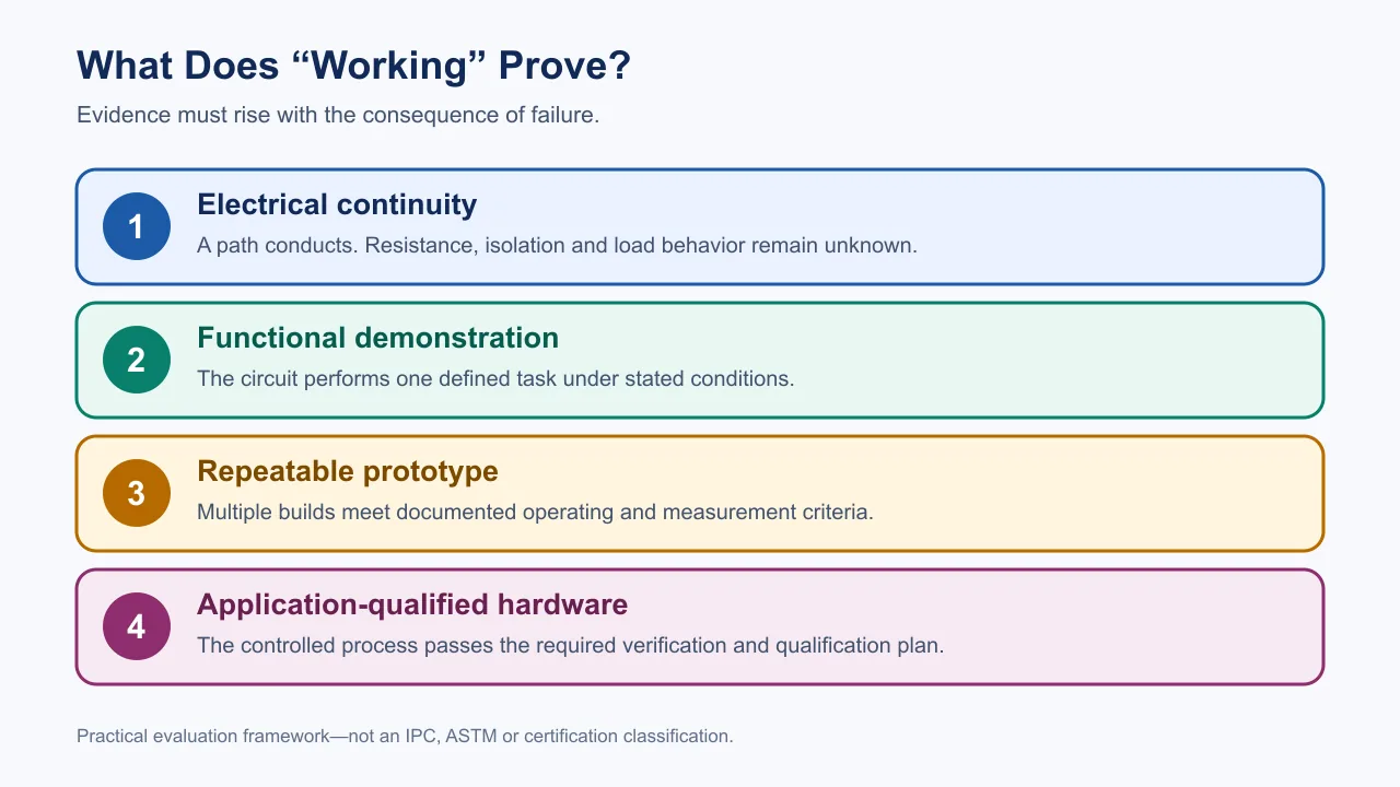
This distinction matters because many online demonstrations establish Level 2 and are then described as though they establish Level 4. The missing evidence may include conductor variation across print directions, contact resistance at component leads, dielectric leakage, thermal cycling and lot-to-lot repeatability.
Which 3D-Printing Routes Can Produce a Functional Circuit?
| Route | What it can do | Main constraint | Evidence to request |
|---|---|---|---|
| Conductive filament | Print simple resistive paths, sensors, passives or low-demand interconnects inside a polymer part. | Resistance, anisotropy, contact quality and nozzle/material contamination. | Printed-direction resistivity, trace geometry, load test and connection method. |
| Deposited conductive ink | Place finer conductors on flat or shaped dielectric surfaces. | Ink/substrate compatibility, wetting, continuity and cure or sinter conditions. | Sheet or bulk resistance after the specified post-process, adhesion and minimum geometry. |
| Printed carrier plus plating or coating | Combine geometric freedom with a metallic conductor layer. | Coverage in recesses, selective metallization, adhesion and plating uniformity. | Cross-sections, continuity through transitions, thickness distribution and environmental adhesion. |
| Multi-material AME | Build dielectric and conductive layers, vias and embedded structures on specialized equipment. | Platform-specific materials, feature rules, assembly window and proprietary process data. | Stack-specific design rules, coupons, thermal history, inspection and reliability results. |
| Hybrid embedded electronics | Pause printing to insert conductors, components or conventional subassemblies. | Registration, contacts, encapsulation stress, repair and thermal exposure. | Placement tolerance, contact retention, encapsulation and functional stress results. |
A “yes” in this table is conditional. For example, the peer-reviewed work by Flowers and colleagues demonstrated printed resistors, capacitors, inductors and a high-pass filter using selected conductive thermoplastics and a modified dual-material printer. It is evidence that functional circuits are possible with that controlled approach—not that every conductive filament behaves like copper.
Why a 3D-Printed Circuit Works Once—and Then Fails
The voltage at the load is too low
Likely mechanism: the printed trace or connection adds more resistance than the circuit budget allows. Check: measure resistance and voltage drop at the actual operating current, including contacts. Response: shorten or widen the path, change its cross-section or orientation, improve the post-process or use a lower-resistance conductor such as plated metal or conventional copper.
The trace becomes hot
Likely mechanism: resistive loss is concentrated in a narrow trace, transition or contact. Check: monitor temperature rise during the intended duty cycle while recording current and voltage. Response: stop before material softening or unsafe temperature is approached; redesign the conductor and confirm the dielectric’s thermal window. Do not copy a universal current rating from an unrelated filament or ink.
The connection is intermittent
Likely mechanism: poor lead contact, print-direction anisotropy, cracks, weak adhesion or deformation. Check: monitor resistance while gently applying the mechanical and thermal conditions expected in use. Response: redesign the termination, use a validated conductive adhesive or metallized pad, add strain relief, or move the vulnerable connection to a conventional PCB.
Adjacent paths leak or short
Likely mechanism: overspray, stringing, conductor migration, dielectric voids, insufficient spacing or contamination. Check: inspect the geometry and measure isolation at a voltage appropriate to the application. Response: correct deposition and cleaning, increase spacing or dielectric thickness, and reprint a coupon before the complete assembly.
The circuit drifts after storage or cycling
Likely mechanism: moisture, oxidation, polymer relaxation, conductor/dielectric expansion mismatch or attachment degradation. Check: repeat the baseline measurements after relevant temperature, humidity, bending or vibration exposure. Response: change material or protection strategy and repeat the test. A single surviving sample is not a process capability result.
How to Test a 3D-Printed Circuit Board Step by Step
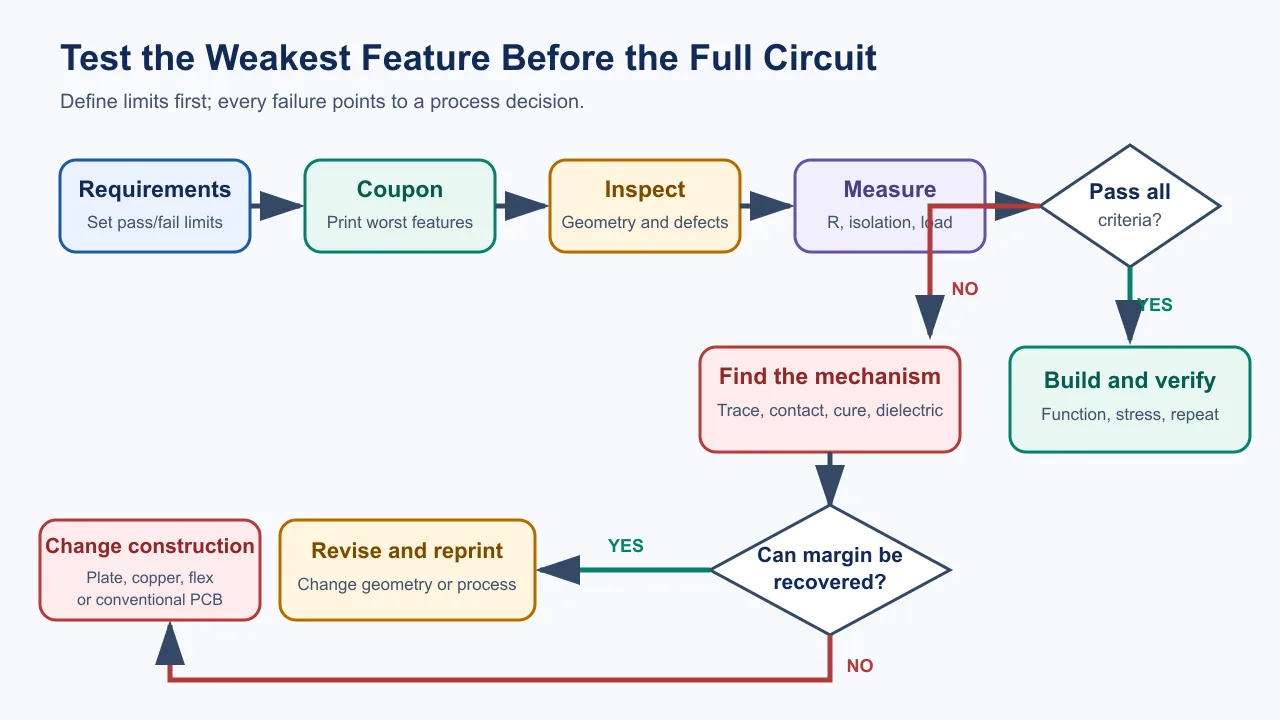
Define pass/fail limits before printing. Those limits must come from the circuit requirement, component data, safety needs and the proposed material stack—not from this general article.
- Freeze the process identity. Record printer, material lots, trace orientation, geometry, deposition settings, cure or sinter recipe, surface preparation and attachment method.
- Print a representative coupon. Include the narrowest trace, longest route, tightest spacing, layer transition, via or vertical path, and the actual termination style.
- Inspect before power. Look for gaps, neck-downs, smearing, voids, unintended bridges, lifted edges and poorly filled transitions. Use magnification or imaging appropriate to the feature.
- Measure continuity and isolation. Verify the intended net and adjacent-net separation. Use a four-wire method when lead and contact resistance would materially distort a low-resistance measurement.
- Run a controlled load test. Increase toward the intended operating condition while observing voltage drop and temperature. Use current limiting and stop rules suitable for the circuit and material.
- Validate attachment. Inspect and measure the transition between printed conductors and components, connectors or conventional copper. Repeat after expected handling.
- Test the intended function. Measure the outputs and margins that matter; “it turns on” is not a complete acceptance criterion.
- Apply relevant stress. Temperature, humidity, flexing, vibration, chemical exposure or storage testing should reflect the use case. Remeasure against the baseline.
- Repeat the build. A viable prototype process must reproduce critical results across more than one specimen. Production or regulated use requires a much stronger, application-specific plan.
What Published Demonstrations Actually Prove
Printed passives and a high-pass filter
A peer-reviewed study in Additive Manufacturing measured several conductive thermoplastics and printed passive components, a filter, a receiver coil and connections to surface-mounted components. It proves: selected materials, geometry and equipment can create measurable functional circuits. It does not prove: that generic carbon-filled filament has copper-like loss, that the process supports ordinary reflow assembly, or that the devices meet an unrelated life requirement.
A coated, printed UV-sensor circuit
A 2024 study reproduced and tested a UV-sensor circuit using 3D-printed polymers, selective conductive coating, commercial components and silver epoxy. It proves: a hybrid printed shape, metallization and component-attachment route can form a functioning sensor. It does not prove: that an uncoated desktop print is a complete PCB or that the construction is qualified for every harsh environment.
NASA’s 3D Printing of Electronics Laboratory
NASA Goddard describes printing custom circuitry and sensors on curved surfaces, rapid prototyping for low-risk missions and spaceflight-specific materials testing. It proves: additive electronics has credible value for unique geometry and early testing. It does not prove: that every printed circuit is flight-qualified; NASA explicitly separates prototyping from mission-specific testing.
When a Conventional PCB or Hybrid Build Is the Better Choice
Choose the construction that meets requirements with defensible margin. Conventional copper is usually the safer baseline when the product needs high current with low loss, tight controlled impedance, fine-pitch assembly, established thermal capability, broad fabrication capacity, repairability or mature qualification evidence. PCBtry’s guide to multilayer PCB manufacturing explains the established route for planar multilayer interconnects.
Do not assume additive electronics is the only way to fit a circuit around a shape. A flex or rigid-flex construction may retain familiar copper conductors and assembly processes while solving packaging constraints; see when to use rigid-flex PCB. A hybrid may also be best: print the structural carrier, use plating or embedded wiring where appropriate, and place the dense or high-stress electronics on a conventional PCB.
| Requirement | First route to evaluate | Reason |
|---|---|---|
| Simple custom sensor or resistive function in a shaped part | Additive or hybrid coupon | Geometry may justify process development. |
| Dense planar digital assembly | Conventional multilayer PCB | Mature feature, assembly and test ecosystem. |
| Circuit must bend or fold predictably | Flex or rigid-flex PCB | Established copper-based bend design may be lower risk. |
| Shaped structure plus dense electronics | Hybrid construction | Uses additive geometry only where it creates value. |
| Safety-critical or long-life harsh service | Qualified construction with application evidence | A demonstration is not enough; the full process needs appropriate qualification. |
Frequently Asked Questions
Can a normal desktop 3D printer make a working circuit board?
It can produce simple conductive paths or a carrier when compatible materials and multiple process steps are used. It generally does not turn ordinary plastic filament into a fine-featured, populated FR-4 replacement in one operation.
Does conductive filament work like copper PCB traces?
No universal comparison is valid. Conductive composites vary widely and can be direction-dependent; measure the printed geometry and contacts under the intended load.
Can you solder components to a 3D-printed circuit?
Sometimes, but the attachment method depends on conductor, substrate and thermal window. Conductive adhesives, sockets, low-temperature processes or later metallization may be used when ordinary soldering would damage the structure.
Can a 3D-printed circuit carry high current?
Only if the specific conductor geometry and contacts meet the allowed voltage-drop and temperature-rise limits. Many conductive polymers are poorly suited to low-loss power paths; test rather than infer from continuity.
Can you print multilayer circuits and vias?
Specialized multi-material and hybrid processes can create multilayer interconnects and vertical transitions. Their design rules and inspection methods are platform-specific.
Is lighting an LED proof that the board works?
It proves a narrow functional demonstration at that moment. It does not prove margin, repeatability, insulation, attachment life or environmental reliability.
How do you measure a printed trace accurately?
Use a method appropriate to its expected resistance and geometry. Four-wire measurement can reduce lead and contact error for low values, while the complete path and terminations still need load testing.
Are 3D-printed circuit boards suitable for RF?
Some additive processes have demonstrated RF structures, but dielectric properties, conductor loss and roughness, geometry, transitions and repeatability must be characterized for the exact stack and frequency.
Are 3D-printed circuits cheaper than traditional PCBs?
Not automatically. Cost depends on equipment, materials, post-processing, yield, inspection, assembly, volume and the value of geometric integration. A fast prototype can still be an expensive production route.
How long does a 3D-printed circuit last?
There is no universal lifetime. It depends on the material stack, conductor, interfaces, protection, load and environment. Use application-relevant testing and process-specific evidence.
Need Help Choosing a Manufacturable Circuit Construction?
Share the geometry, stack requirements, current and voltage, component pitch, environment, expected volume and validation target with PCBtry. We can help compare conventional rigid, flex, rigid-flex and hybrid PCB options. Capability for a specialized additive-electronics process should be confirmed separately for the exact material and equipment.
A 3D-printed circuit can be genuinely functional. The engineering mistake is to treat every form of function as equal. Define the acceptance criteria first, test the weakest representative features, and increase the evidence level only when the measurements support it. If additive geometry creates no product value—or the electrical and reliability margins remain uncertain—a conventional or hybrid copper construction is often the better decision.



0 Comments