




An FPGA is not an alternative to a PCB. A field-programmable gate array is an integrated circuit whose digital logic can be configured after manufacturing. A printed circuit board is the physical platform that mounts the FPGA and other components, distributes power, and connects signals. In a real product, the FPGA usually sits on a PCB, so the useful decision is not “FPGA or PCB?” but “Which FPGA implementation path and which board architecture fit the project?”
FPGA vs PCB: The Short Answer
An FPGA performs configurable digital functions inside one semiconductor package. A PCB creates the physical electrical and mechanical system around that package. Rebuilding an FPGA configuration can change the device’s digital behavior without changing the bare board, provided the existing pins, power system, clocks, memory and interfaces still support the new design. Changing PCB connectivity, stackup, component placement or form factor normally requires a new board revision and manufacturing cycle.
The terms are easy to confuse because an “FPGA board” contains both. It is a PCB populated with an FPGA plus the supporting power regulators, oscillators, configuration path, connectors and often memory or communication devices.
FPGA vs PCB Comparison Table
| Decision point | FPGA | PCB |
|---|---|---|
| What it is | A configurable integrated circuit | A manufactured board that mechanically supports and electrically interconnects components |
| Main job | Implements digital logic, interfaces and data paths defined by a configuration | Distributes power and carries signals among the FPGA, memory, connectors and other components |
| How behavior changes | Update the verified FPGA configuration when the existing hardware supports it | Revise schematic, layout, stackup or components and fabricate/assemble another board revision |
| Typical design inputs | HDL or generated logic, IP configuration, timing and physical constraints, pin assignments | Schematic, component data, netlist, placement, routing, stackup and fabrication/assembly outputs |
| Verification focus | Functional simulation, synthesis checks, timing closure and on-hardware validation | ERC/DRC, signal and power integrity where required, DFM, inspection and electrical test |
| Cost drivers | Device family, capacity, package, speed grade, transceivers, memory and tool/IP choices | Board size, layer count, materials, feature sizes, via structure, finishes, assembly and test |
| Common failure boundary | Logic, timing, constraints, clocking or configuration errors | Power integrity, signal integrity, routing, footprint, assembly or fabrication errors |
This table does not identify a universal winner because the two items solve different layers of the same system. An FPGA can be replaced by a different processing device in some architectures, but the system still needs a physical interconnect platform. Likewise, a PCB does not acquire programmable logic merely because an FPGA could be mounted on it.
What an FPGA Does
An FPGA contains configurable logic resources and programmable interconnect. Depending on the selected family, it may also contain dedicated memory blocks, arithmetic resources, clock-management circuits, high-speed transceivers or hard processor functions. The exact resource mix is device-specific; “FPGA” alone does not prove that a design supports a particular interface, throughput or processing load.
Designers describe and constrain the intended hardware, then use vendor tools to synthesize, place and route the design inside the FPGA fabric. The resulting configuration data controls how the available resources are connected. This is different from software running sequentially on a fixed processor architecture, although an FPGA design may include processor cores and software as part of the system.
Reconfigurability is valuable for prototyping, parallel digital processing, custom interfaces and products that may need logic updates. It is not permission to ignore the physical board. A new configuration can increase switching activity, use different I/O banks or activate different transceivers, which may change power, thermal and signal-integrity demands even when the PCB is unchanged.
What a PCB Does
A PCB supplies the physical foundation for the complete electronic assembly. Copper features connect component pins; dielectric layers and reference planes shape signal return paths; power structures distribute current; pads and holes enable assembly; and the board outline, mounting features and connectors define mechanical integration.
For an FPGA system, the board must support the selected package and its escape routing, every required supply rail, decoupling network, clocks, reset and configuration access. It may also connect external memory, analog conversion, sensors, network interfaces or high-speed connectors. The correct stackup and routing rules depend on the actual interfaces, package, material system and fabricator capabilities—not on the word “FPGA.”
If the design includes fast edge rates, controlled-impedance channels or dense BGA routing, the board team may need signal-integrity, power-integrity and manufacturing input early. PCBtry’s guide to high-frequency PCB design guidelines explains why stackup, reference planes and routing constraints must be treated as one system rather than independent checklist items.
How an FPGA and PCB Work Together
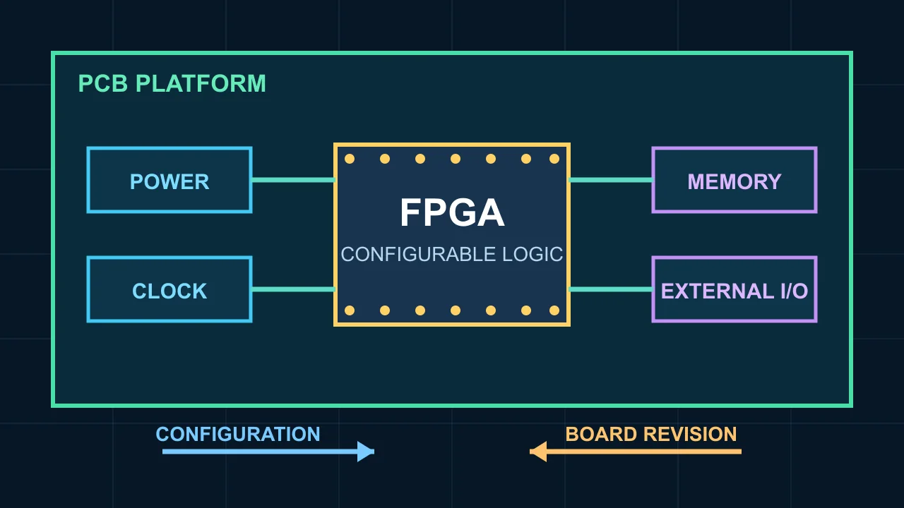
The FPGA is one node in a board-level network. Regulators convert the input supply into the rails required by the selected device. Decoupling components provide local transient current paths. Oscillators or clock devices provide timing references. A configuration source or host loads the required data according to the device’s supported modes. Memory and peripherals exchange signals through assigned I/O banks or dedicated interfaces.
That relationship creates a two-way dependency. The logical design needs pins with compatible standards, bank voltages and dedicated resources. The PCB needs an assignment that can be routed with acceptable reference paths, spacing, length relationships and connector mapping. A pinout that is legal inside the FPGA can still be difficult to route on the board, while a visually convenient PCB swap can violate FPGA bank, clock or differential-pair rules.
A useful design review therefore traces each important interface across four boundaries: FPGA resource, package pin, PCB interconnect and receiving device. This makes it easier to detect a mismatch that would be invisible if the FPGA and PCB were reviewed separately.
FPGA Development Board vs Carrier Board vs Custom PCB
| Hardware path | Best fit | Main advantage | Key limitation to verify |
|---|---|---|---|
| FPGA development board | Learning, algorithm proof, interface experiments and early firmware/logic work | Known board with power, configuration and common peripherals already implemented | Form factor, connectors, I/O voltage, memory and lifecycle may not match the product |
| Development board plus carrier PCB | Prototype needing custom connectors, sensors or power around a proven module | Reduces the first custom board’s FPGA-package and power complexity | Extra connectors, size and module availability can constrain production |
| Fully custom FPGA PCB | Product-specific size, interfaces, power, thermal, cost or qualification requirements | Board architecture can be optimized around the actual system | Requires device-specific schematic, layout, bring-up and manufacturing validation |
Start with a development board when the main uncertainty is the logic, resource fit or interface concept. Consider a carrier when the development board remains suitable but the product needs custom external connectivity. Move to a custom board when the module prevents required form factor, power, thermal, interface, lifecycle or production objectives. There is no reliable universal production-volume threshold because engineering effort, module cost, qualification burden and supply risk vary by project.
When the custom design is still being stabilized, a prototype build can test assembly, power-up and interfaces before a larger order. See PCBtry’s prototype PCB DFM and quote checks for the board files and evidence that should accompany that step.
Board-Level Design Challenges Around an FPGA
Power rails, sequencing and decoupling
Many FPGA families require multiple supplies, but their voltage, tolerance, sequencing and ramp requirements are device-specific. Use the current device data sheet, pin-connection guide and board-design guide. Estimate power using the intended resource utilization and operating conditions, then verify regulator capacity, transient response, decoupling placement, return paths and thermal margin. Do not copy a regulator or capacitor set from another FPGA board without confirming the package and operating case.
I/O banks and pin assignment
Pin planning must respect bank voltage, I/O standard, differential pairing, clock-capable pins, transceiver locations, configuration pins and package restrictions. The board view adds connector order, component placement, via escape and routing congestion. Freeze assignments only after both FPGA implementation checks and PCB routing checks have been performed.
Clocks, memory and high-speed channels
Clock quality, return paths, termination and coupling can affect whether an interface works reliably. External memory and serial transceivers introduce device-specific topology, loss, timing and reference-clock requirements. The correct trace geometry comes from the chosen stackup. If impedance is controlled, define how it will be verified; PCBtry’s guide on measuring PCB trace impedance covers coupons and TDR evidence.
Package escape, thermal path and test access
A dense BGA may drive layer count, via technology, fanout style and inspection strategy. Power dissipation must travel through the package, board and any heat-spreading hardware to the environment. Bring-up also needs safe access to configuration, reset, power rails and diagnostic signals. Resolve these needs before routing consumes the available space.
FPGA Design Flow vs PCB Design Flow
The two flows share terms such as “constraints” and “place and route,” but the objects are different. FPGA place and route maps logical functions and programmable connections inside the device. PCB place and route positions physical components and creates copper interconnect on a manufactured board.
- System definition: establish interfaces, data rates, latency, power, environmental and lifecycle requirements.
- Device and package selection: confirm logic resources, I/O, banks, transceivers, memory, package escape and availability.
- Joint pin planning: reconcile internal FPGA resource rules with PCB placement and routing.
- FPGA implementation: synthesize, implement and check functional and timing constraints.
- PCB implementation: complete schematic, stackup, placement, routing, analysis and DFM using the validated pin map.
- Cross-domain change control: revalidate both flows whenever a pin, interface, package, clock or power assumption changes.
- Build and bring-up: inspect and electrically test the assembly, verify rails and clocks safely, configure the FPGA and validate interfaces.
Typical FPGA outputs include configuration data, programming instructions, constraints and pin-assignment exports. PCB manufacturing outputs include fabrication data, drill data, drawings, stackup notes, assembly data and a bill of materials. A complete handoff also preserves the approved mapping between FPGA signals, package pins and PCB nets.
Engineering Scenario: Pin Planning Connects Both Domains
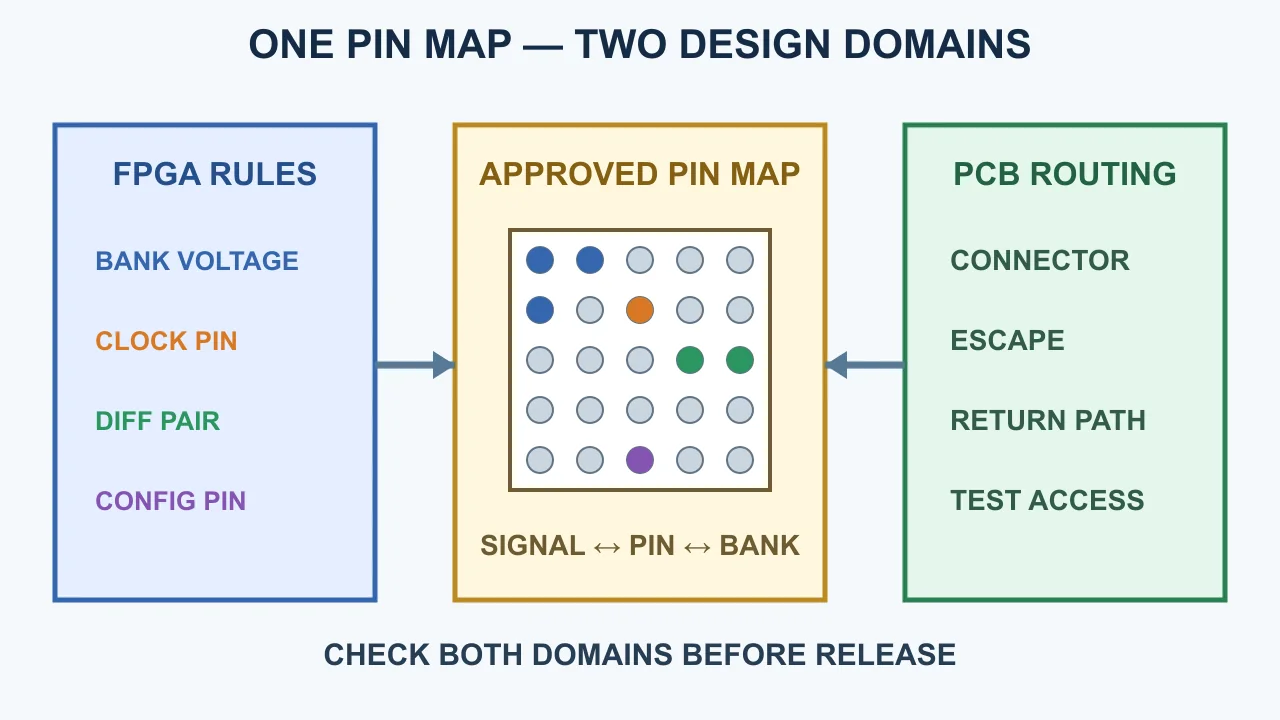
AMD’s published Vivado I/O and clock-planning guide describes a recurring integration problem: a non-optimal FPGA pinout can delay board layout and make timing or signal-integrity goals harder to meet. This is not a PCBtry customer case. It is a documented vendor workflow illustrating why FPGA and PCB decisions must be coordinated.
Problem: if pin assignments are made from only the logical view, external connections may cross, PCB traces may lengthen, or required FPGA resources may conflict with the convenient board route. Treatment: consider data flow from the PCB through the package to the FPGA die and analyze connectivity jointly. Action: FPGA, PCB and system designers review I/O standards, banks, clocks, differential pairs, power/ground availability, decoupling and programming/debug access before finalizing assignments. Published result: AMD states that this approach can reduce internal and external trace lengths and routing congestion. Reader lesson: pin planning is a controlled interface between two design domains, not a one-time spreadsheet export.
The result is directional, not a guaranteed numerical improvement. The actual benefit depends on the selected device, package, interfaces, placement and constraints.
Decision Guide: Which Hardware Path Fits Your Project?
| If this is your main condition | Start with | Evidence needed before advancing |
|---|---|---|
| You are learning FPGA tools or proving logic feasibility | Development board | Resource fit, timing feasibility and working interface demonstration |
| You need custom connectors or sensors but can retain the module | Carrier PCB | Module pinout, electrical levels, mechanical constraints and supply plan |
| Size, power, thermal or interfaces cannot be met by a module | Custom FPGA PCB | Selected device/package, validated pin plan, power estimate, interface constraints and stackup concept |
| You need production qualification or long lifecycle control | Custom architecture review | Availability, revision control, test strategy, environmental requirements and supplier capability confirmation |
Do not choose a custom board merely because it appears more professional. Choose it when system requirements justify ownership of the additional design, verification, fabrication, assembly and bring-up work.
FPGA-Based PCB Planning Checklist
This is original general planning guidance, not a device-vendor checklist, factory record or substitute for the selected FPGA documentation.
- Record the exact FPGA part number, package, speed grade and approved alternatives.
- List required logic resources, memory, transceivers, clocks and external interfaces.
- Confirm every supply rail, tolerance, sequence and estimated current case.
- Map I/O standards and bank voltages before fixing the connector pinout.
- Identify dedicated clock, configuration, reset, JTAG and special-function pins.
- Export and revision-control the FPGA-to-PCB pin map.
- Define memory and high-speed interface topology from current vendor guidance.
- Develop the stackup with the intended fabricator before final impedance routing.
- Check BGA fanout, via technology, assembly clearances and inspection access.
- Estimate dissipation and define the board-to-environment thermal path.
- Provide test points or safe measurement access for rails, clocks, reset and configuration.
- Re-run FPGA and PCB checks after every cross-domain pin or interface change.
Frequently Asked Questions About FPGA vs PCB
Is an FPGA the same as a PCB?
No. An FPGA is a configurable integrated circuit. A PCB is the physical board that mounts and interconnects electronic components, including an FPGA when the design uses one.
Can an FPGA replace a PCB?
No. An FPGA may consolidate digital logic that otherwise needs multiple devices, but it still needs power, physical connections and usually a PCB or another package-level interconnect platform.
Is an FPGA development board a PCB?
Yes. It is an assembled PCB designed around an FPGA and supporting components. The board is the complete platform; the FPGA is one component on it.
Can FPGA logic be changed without redesigning the PCB?
Sometimes. A configuration update can change logic while retaining the board, but only if the existing device resources, pinout, power, clocks, memory, thermal path and external interfaces support the change.
What is the difference between programming an FPGA and designing a PCB?
FPGA work defines and verifies configurable hardware inside the device. PCB work defines the schematic, component placement, stackup and copper connections that will be physically manufactured and assembled.
Do all FPGA projects need a custom PCB?
No. Learning and early proof work often use a development board. A carrier or custom PCB becomes useful when interfaces, form factor, power, thermal, cost, lifecycle or qualification needs cannot be met by the existing board.
Why are FPGA PCBs often multilayer?
Many FPGA systems need dense BGA escape routing, several power rails, reference planes and controlled high-speed paths. Those needs can drive a multilayer design, but the required layer count must be developed from the actual package, interfaces and routing density.
What files does a PCB manufacturer need for an FPGA board?
The exact package depends on scope, but fabrication commonly needs board fabrication data, drill data, drawings and stackup notes; assembly adds BOM and placement data. Controlled interfaces, impedance requirements and special via structures must be clearly documented.
Can a PCB manufacturer program the FPGA?
Programming is a separate service and cannot be assumed. Confirm whether the assembler supports the selected device and method, then provide controlled configuration files, instructions, fixtures or cables, acceptance criteria and revision identification.
What should be checked first on a new FPGA PCB?
Use a safe device-specific bring-up plan. Common early checks include shorts, rail values and sequencing, current behavior, reset, clocks and configuration access before enabling or exercising high-speed interfaces.
Plan Your FPGA PCB With Verified Inputs
Before requesting a PCB review or quotation, provide the exact FPGA/package, schematic, preliminary stackup, board dimensions, interface list, controlled-impedance requirements, BGA/via constraints, expected assembly scope and test expectations. Ask the supplier to confirm which fabrication, assembly, inspection and programming capabilities are actually available for that design. Device-specific electrical sign-off remains the responsibility of the qualified design team.
Technical Sources and Boundaries
- Microchip: What Is an FPGA? — FPGA definition and design-flow overview.
- AMD UG899: I/O and Clock Planning — cross-domain pin-planning scenario and stated routing benefits.
- Microchip PolarFire SoC FPGA Board Design Guidelines — examples of device-specific board topics and checklists.
- Intel Agilex 5 PCB Design Guidelines — package, interface and power-distribution topics.
All voltage, current, sequencing, decoupling, timing, impedance, thermal and layout values must come from the current documentation for the selected device and the qualified PCB stackup. This article provides a decision framework, not universal design limits.



0 Comments