




Hot-Swap PCB vs Soldered PCB: Quick Answer
A hot-swap keyboard PCB holds each removable mechanical switch in a purpose-designed socket. A soldered keyboard PCB connects each switch pin directly to a soldered through-hole joint. The practical difference is therefore not whether solder exists anywhere on the board: hot-swap sockets themselves are normally soldered to PCB lands. The difference is the interface a user opens when replacing a switch.
Choose hot-swap when quick switch experiments, easy field replacement, and a low barrier for beginners matter most. Choose soldered when the product needs a fixed switch population, alternative switch positions in one footprint, or the simplest direct connection between switch pins and PCB pads. Neither architecture is automatically more reliable, quieter, cheaper, or compatible with more switches; those outcomes depend on the selected parts and the complete keyboard design.
In this article, “normal PCB” means a soldered-switch mechanical-keyboard PCB. It does not mean a powered backplane designed for live insertion. Disconnect the keyboard before changing switches unless the finished product’s instructions explicitly permit powered servicing.
Hot-Swap PCB vs Soldered PCB Comparison Table
| Decision factor | Hot-swap keyboard PCB | Soldered keyboard PCB |
|---|---|---|
| Switch replacement | Pull and insert a compatible switch without desoldering | Desolder the old switch and solder the replacement |
| User skill | Lower barrier for routine switch changes | Requires controlled soldering and desoldering |
| Electrical interface | Switch pin contacts a socket; socket is soldered to PCB lands | Switch pin is soldered directly to a plated hole/pad |
| Layout options | Commonly locks each socket to one physical switch position | Can support multiple positions if the PCB footprint and plate are designed for them |
| Compatibility | Must match switch technology, pin geometry, socket, footprint, plate, and clearance | Must match switch technology, pin geometry, hole pattern, plate, and clearance |
| Typical handling risk | Bent pin, incomplete seating, damaged contact, cracked socket joint, or lifted socket land | Cold joint, excess heat, bridged joint, damaged barrel/pad, or rework damage |
| Production inputs | Socket BOM, placement, soldering, inspection, and insertion-support plan | Through-hole insertion, soldering, lead trimming if applicable, and joint inspection |
| Field repair | Faster when the switch is the failed item; socket faults still require board work | Slower switch replacement but direct joints are straightforward to inspect |
| Cost | Depends on socket price, assembly route, yield, and service strategy | Depends on labor, selective/wave/hand-solder route, variants, and rework |
| Best fit | Enthusiast products, switch trials, education, and easy field replacement | Stable configurations, layout-flexible kits, and products where switch changes are rare |
The table is a starting point, not a universal verdict. A well-designed soldered PCB can be easier to service than a poorly supported hot-swap PCB, while a carefully integrated socket can make switch replacement far less disruptive than repeated desoldering.
What Changes Electrically and Mechanically?
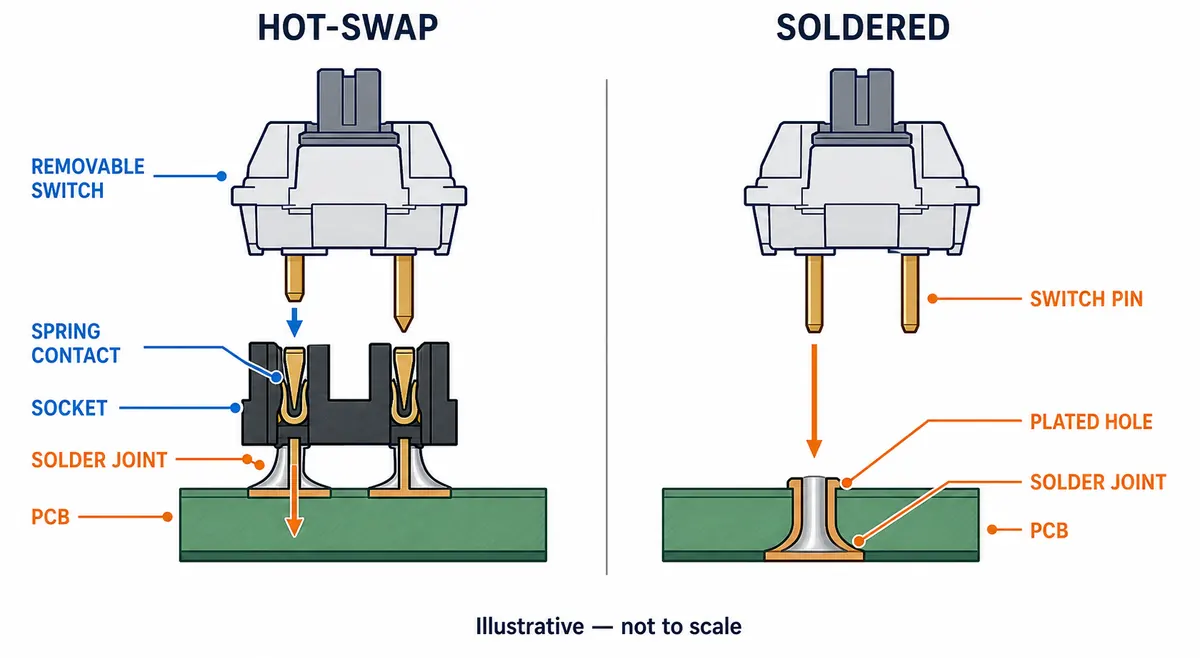
Hot-swap adds a removable switch-to-socket contact; soldered construction joins the switch pin directly at the plated hole. Illustrative, not to scale.
With a soldered design, the metal switch pin passes through the PCB and becomes part of a solder joint. That joint provides the electrical connection and mechanically retains the pin. Replacing the switch means heating and removing that joint without damaging the plated hole or surrounding laminate.
With a hot-swap design, the switch pin enters a spring-contact socket. The socket terminals are then soldered to copper lands on the PCB. This adds an interface: switch pin to socket contact, followed by socket terminal to solder joint and PCB copper. It also transfers insertion and extraction force through the socket and its PCB attachment.
That distinction explains both the convenience and the design responsibility. Hot-swap removes soldering from the routine switch-change operation, but it does not remove solder-joint design, land-pattern accuracy, component placement, inspection, or mechanical support from manufacturing. For the implementation details, see PCBtry’s guide to making a PCB hot-swappable.
Switch Replacement and Builder Skill
For a compatible hot-swap board, a user can remove a keycap, pull the switch, inspect and straighten the replacement pins, align them with the socket, and press the switch into place. No soldering iron is needed for that normal replacement. The board should be unpowered and supported so insertion force does not flex the PCB or peel the socket away from its lands.
Replacing a soldered switch involves disassembly, controlled heating, solder removal, extraction, hole cleaning, installation, resoldering, and inspection. The work is manageable for a trained builder, but each heat cycle creates an opportunity to damage a pad, plated barrel, nearby component, or solder mask. A repair plan should specify temperature control, dwell discipline, ESD precautions, and acceptance criteria rather than treating desoldering as a casual step.
Hot-swap is therefore more accessible for frequent experimentation. Soldered construction is reasonable when switches are selected once and expected to remain in service, or when the builder already has suitable rework tools and skills.
Compatibility: Switch, Socket, Footprint and Plate
“Hot-swappable” does not mean “accepts every keyboard switch.” Verify the complete compatibility stack:
- Switch technology: mechanical-contact, optical, and magnetic/Hall-effect switches use different sensing arrangements and are not interchangeable merely because their housings look similar.
- Pin and post geometry: compare the exact switch drawing with the socket or PCB drawing. Do not rely only on a marketplace label such as “MX compatible.”
- Socket family and part number: different socket versions can have different outlines, terminal geometry, ratings, or recommended layouts.
- PCB footprint: land dimensions, openings, solder-mask clearances, orientation, and nearby routing must match the selected part’s current documentation.
- Plate and case: the plate cutout, thickness, switch orientation, stabilizers, component height, and underside clearance must work as a system.
PCB-mount switches may include extra plastic locating posts, while plate-mount variants may omit them. Whether both work depends on the PCB holes and the plate—not on the hot-swap label alone. The same caution applies to north-facing and south-facing LED orientation; PCB orientation can affect component and keycap clearance, which is explained in What Is a South-Facing PCB?.
Layout Flexibility and Product Variants
Many socket footprints occupy a fixed position and a substantial area on the PCB. That can make it difficult to place two socket positions close enough to support alternative bottom rows, split backspace, stepped Caps Lock, or ISO/ANSI choices on one board. It may also constrain diode, LED, and trace placement.
A soldered PCB can use overlapping through-hole switch positions when the electrical and mechanical design allows it. This can help a kit support several layouts with one PCB. However, soldered does not automatically mean layout-flexible: the designer still has to create the alternative holes, nets, plate options, firmware matrix, and assembly documentation.
For a production keyboard with one fixed layout, socket position rigidity may be irrelevant. For a configurable kit, layout support can outweigh the convenience of tool-free switch replacement. Decide the layout matrix before choosing the connection method, not after routing is complete.
Reliability and Failure Boundaries
There is no defensible universal answer to “Which lasts longer?” without naming the exact switch, socket, PCB, assembly process, usage profile, and failure criterion.
Hot-swap designs add contact and mechanical interfaces. Plausible failure paths include a bent switch pin missing the socket contact, incomplete seating, contamination, contact wear, a cracked socket solder joint, or a peeled land after unsupported insertion. Soldered designs avoid the removable socket contact, but replacement creates thermal and mechanical rework risk. Plausible failures include a poor solder joint, a damaged plated hole, lifted copper, or excessive heat applied during desoldering.
Component ratings must remain part-specific. For example, a Kailh specification for part CPG151101S11 Rev. A describes a 100-cycle minimum life test under its stated conditions. That figure belongs to that exact document and revision; it must not be generalized to every Kailh version, every socket family, or every finished keyboard. Newer or different parts may have different specifications. Always use the datasheet tied to the purchased manufacturer part number and revision.
For either architecture, reliability improves when the PCB land pattern, material, copper geometry, solder profile, inspection method, plate support, and user instructions are designed together. Functional matrix testing should follow assembly and any switch replacement.
Assembly, Repair and Cost Drivers
Hot-swap is not automatically the expensive option, and soldered is not automatically the cheap one. Request a quotation using the actual design and volume. Important cost drivers include:
- socket unit price and supply continuity;
- SMT placement, paste-aperture development, reflow, and automated optical inspection;
- through-hole insertion and hand, wave, or selective soldering labor;
- PCB area and routing complexity created by the footprint;
- plate, fixture, underside-support, and final assembly requirements;
- expected yield, rework access, spare-parts policy, and warranty handling;
- number of layout or switch variants needed across the product line.
Field-service economics can reverse the initial comparison. A replaceable switch may reduce service time when switches are expected to change, but a damaged socket still requires solder rework. A soldered product may have fewer connector interfaces, yet one switch replacement takes longer. Calculate total cost around the anticipated failure and service model instead of comparing bare PCB prices.
Does Hot-Swap Change Keyboard Sound or Feel?
Hot-swap architecture alone does not guarantee a particular sound or key feel. Switch construction, plate material and thickness, mounting style, case stiffness, foam, stabilizers, keycaps, PCB flex, and assembly tolerances can all change the result. Two keyboards that differ in several of those variables cannot isolate the effect of the switch connection method.
If sound or feel is a purchase requirement, compare otherwise matched builds or test prototypes with controlled variables. Treat descriptions such as “hot-swap always sounds hollow” or “soldered always feels firmer” as unverified generalizations unless a repeatable, controlled test supports them.
Engineering Scenario: Preventing Socket and Pad Damage
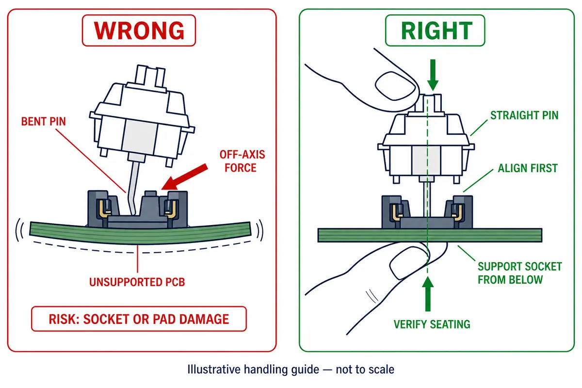
Inspect and align the pin, then support the socket from below during insertion. Illustrative handling guide, not to scale.
Keebio’s public Iris Rev. 6–8 build documentation describes a concrete integration problem: a slightly misaligned switch pin can push a hot-swap socket off-center and tear it from the PCB. Its instructions tell builders to support the socket from below during insertion, avoid inserting switches with bent pins, and use a tray liner that supports the sockets.
This is not presented as a PCBtry customer case, and it does not prove that every socket or board fails in the same way. It is a traceable example of how the load path matters:
| Observed risk | Mechanism | Preventive control | Verification |
|---|---|---|---|
| Bent pin does not enter contact opening | Off-axis force reaches socket body and PCB land | Inspect and straighten or replace the switch before insertion | Visual check before seating |
| PCB flexes during insertion | Local bending increases joint and land stress | Support the PCB/socket underside close to the insertion point | Confirm the board does not visibly bow |
| Switch is partly seated | Pin-contact engagement may be incomplete | Align through plate and socket, then seat evenly | Inspect height and run a key-matrix test |
| Socket joint is damaged | Electrical intermittency or open circuit | Stop repeated insertion; inspect joint and copper before repair | Magnified inspection plus continuity/function test |
The design lesson is broader than the assembly instruction. Review land geometry, copper anchoring permitted by the manufacturer footprint, plate-to-PCB spacing, underside clearance, support features, and servicing access as one mechanical system. Do not “strengthen” a footprint by changing manufacturer-recommended geometry without validation.
Source: Keebio Iris Rev. 6–8 Hotswap build documentation.
Which PCB Should You Choose?
Choose a hot-swap PCB when:
- users will compare or replace switches frequently;
- beginners need routine replacement without soldering tools;
- fast switch-level field service is a product requirement;
- the intended layout is fixed and compatible with the selected socket;
- the mechanical design can support the socket during insertion.
Choose a soldered PCB when:
- the switch configuration will remain stable;
- one PCB must support several overlapping switch positions;
- the product team prefers a direct soldered switch connection;
- trained assembly and rework capability is available;
- socket supply, space, or assembly constraints outweigh tool-free replacement.
Consider offering separate variants if both user groups are commercially important. For a broader view of the board’s role in the product, see What Is a Mechanical Keyboard PCB?.
Hot-Swap vs Soldered PCB Selection Checklist
Saveable checklist: copy or print these 12 checks before releasing the schematic or buying a keyboard.
Download the Hot-Swap vs Soldered PCB Selection Checklist (PDF)
- “Hot-swap” refers to removable keyboard switches, not powered card insertion.
- The exact switch technology matches the sensing circuit.
- Switch-pin and locating-post geometry match the socket or PCB holes.
- The manufacturer part number and current datasheet are fixed in the BOM.
- The PCB footprint matches the selected part and revision.
- Plate cutouts, stabilizers, orientation, and case clearance are compatible.
- Every required layout position is supported by both PCB and plate.
- The board and socket can be supported during switch insertion.
- Assembly inspection covers solder joints, socket alignment, and contamination.
- Functional testing covers every key after assembly or repair.
- Replacement instructions include power-off, pin inspection, and straight insertion.
- Cost comparison includes assembly, yield, repair, variants, and warranty—not just the bare PCB.
This checklist and its two-page printable PDF are original decision aids derived from the verified design factors above. The PDF states its purpose, boundaries, and source links. Neither version is a manufacturer test standard, qualification record, customer file, or substitute for the selected component’s documentation.
Frequently Asked Questions
Is a hot-swap PCB the same as a solderless PCB?
No. The user can normally replace compatible switches without soldering, but the hot-swap sockets and other components are still soldered to the PCB during manufacturing.
Can I put any mechanical switch in a hot-swap PCB?
No. Match the exact switch technology, pins, posts, socket, footprint, plate, orientation, and clearance. Optical and magnetic switches are not automatically compatible with mechanical-switch sockets.
Are five-pin switches compatible with every hot-swap PCB?
No. A board needs the appropriate locating holes and plate geometry. Check the specific PCB and switch documentation; do not rely only on a “five-pin” product label.
Is a hot-swap PCB less reliable than a soldered PCB?
Not inherently. The architectures have different failure paths. Reliability depends on component selection, land pattern, assembly quality, mechanical support, environment, and how often switches are serviced.
How many times can I replace a hot-swap switch?
Use the life specification for the exact socket part number and revision. Do not apply one online cycle figure to all sockets or finished keyboards, and treat damaged or contaminated contacts as a reason to inspect rather than keep cycling.
Should I change switches while the keyboard is connected?
The safest default is no. Disconnect power before insertion or removal unless the product manufacturer explicitly documents a powered procedure. Keyboard “hot-swap” mainly describes solder-free switch replacement.
Does a soldered PCB support more keyboard layouts?
It can, because designers may overlap multiple through-hole switch positions. Actual support still depends on the PCB footprint, plate, stabilizers, matrix, and firmware.
Does hot-swap make a keyboard sound worse?
There is no universal result. Sound depends on the entire keyboard system. Compare otherwise matched prototypes if sound is an acceptance requirement.
Can a damaged hot-swap socket be repaired?
Sometimes, but repairability depends on whether only the solder joint failed or the copper land and laminate were damaged. Inspect first; pad or trace damage may require a qualified board-level repair.
Which type is better for a first mechanical-keyboard build?
Hot-swap is usually easier when a beginner wants to try switches without soldering. A soldered kit is appropriate when learning soldering is part of the goal and the builder has suitable tools and supervision.
Plan the Right Keyboard PCB with PCBtry
The useful question is not simply “hot-swap or normal?” It is which connection method fits the required switches, layouts, service model, production volume, mechanical stack, and verification plan.
Send PCBtry the intended switch and socket part numbers, keyboard layout matrix, plate drawing, stack-up constraints, target quantity, and inspection requirements. The team can review the PCB manufacturing inputs and help identify questions to resolve before quotation. Final compatibility and process acceptance should be tied to approved drawings, samples, and the selected component documentation.



0 Comments