




What Is the Heavy Copper PCB Testing Process?
The heavy copper PCB testing process verifies that thick conductors, plated holes, dielectric structures and finished circuits match the released design and can support the project’s electrical and thermal requirements. It combines dimensional and cross-sectional inspection, continuity and isolation testing, low-resistance measurement, current/temperature-rise validation and any reliability testing required by the application. A standard bare-board electrical test is necessary, but it cannot prove copper thickness, hole-wall quality or temperature rise under load by itself.
PCBTRY supports heavy-copper projects with DFM review, fabrication, inspection and test planning. For an engineering assessment, send Gerber or ODB++ data, drill files, stack-up, finished copper requirements, current paths, allowable temperature rise, quantity and acceptance criteria through our contact page. The test plan should be agreed before production so coupons, sample sizes and reports are built into the order.
How Does the Heavy Copper PCB Testing Process Work?
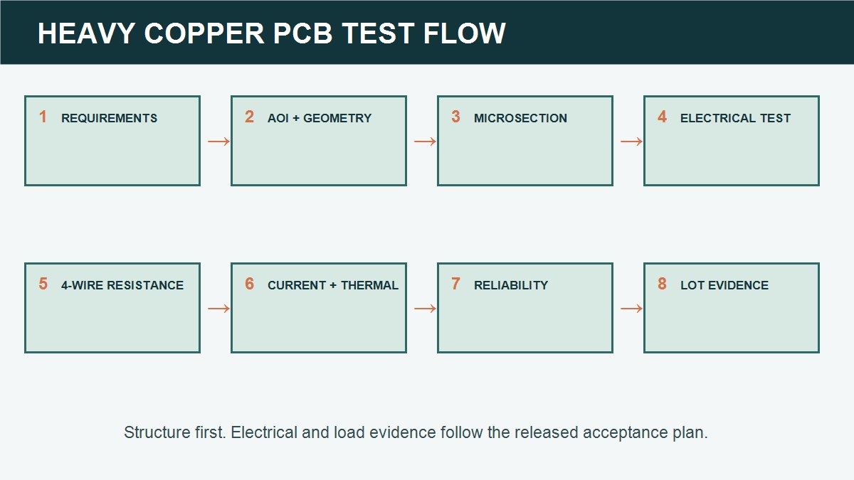
A useful heavy-copper test flow begins with the released requirements, checks the structure while defects are still visible, verifies the finished netlist, then applies current, thermal or environmental stress only where the product requirement calls for it.
1. Review the specification and acceptance plan. Engineering confirms finished copper, conductor width, spacing, plated-hole requirements, stack-up, netlist, current paths, test voltage, temperature limits and required reports. Without an agreed acceptance basis, a measurement has no reliable pass/fail meaning.
2. Verify incoming materials and process coupons. Material identity, base copper and laminate data are checked against the released build. Coupons are placed so the factory can evaluate plating, etch profile, registration or thermal performance without destroying every production board.
3. Inspect conductor imaging and etching. AOI and dimensional measurements look for opens, shorts, neck-downs, residual copper and spacing loss. Thick copper requires deeper etching, which can create sidewall taper and larger finished-feature variation than the artwork suggests.
4. Measure copper and hole structures. Microsections, calibrated thickness methods and applicable surface measurements verify conductor geometry, copper distribution, dielectric separation and plated-hole interfaces. The method must match the feature: an exposed surface reading cannot substitute for an internal cross-section.
5. Run final continuity and isolation tests. Flying probe or fixture testing compares the bare board with the approved net data. This catches connection errors, but not every marginal cross-section or high-resistance power path.
6. Measure critical-path resistance. Low-resistance power conductors may need a four-wire Kelvin method so lead and contact resistance do not dominate the reading. Test points, path length and temperature should be defined because copper resistance changes with geometry and temperature.
7. Validate current and temperature rise. A controlled fixture drives the specified current while temperatures are measured at agreed locations under defined ambient, airflow, duty cycle and mounting conditions. The test validates a particular setup; it is not a universal current rating for the board.
8. Complete reliability evidence and release review. When required, thermal cycling, thermal shock, insulation, solderability or other product-specific tests are performed on defined samples. The final report links results, coupons and deviations to the released lot.
Which Measurements Verify Heavy Copper Geometry?
Heavy copper geometry must be measured after processing because finished width, spacing and sidewall shape can differ from the design artwork. The correct method depends on whether the feature is external, internal, exposed or buried.
| Measurement | What it checks | Typical evidence | Main limitation |
|---|---|---|---|
| AOI / optical dimension | Pattern integrity, width, spacing and visible defects | AOI record or dimensional report | Does not show buried copper thickness or internal interfaces |
| Microsection | Finished copper profile, dielectric spacing and interfaces | Photomicrograph with calibrated dimensions | Destructive and based on defined sampling locations |
| Surface thickness measurement | Accessible outer copper or finish when method is suitable | Instrument reading and calibration reference | May not represent internal layers or local distribution |
| Finished-board thickness | Total construction and local build variation | Thickness report | Cannot separate copper from dielectric contributions alone |
Ask for the measurement location and method, not only a number labeled “copper thickness.” For design context, see PCBTRY’s FR-4 PCB copper thickness guide.
How Are Plated Holes and Copper Interfaces Checked?
Plated holes are checked with cross-sectional evidence because continuity alone can pass through a thin, rough or poorly bonded barrel. A representative microsection can show hole-wall preparation, copper distribution, corner condition, internal-layer connection, voids and resin condition.
The drawing or purchase specification should identify the required finished hole and plating acceptance basis. For power vias, also review drill diameter, annular geometry, copper balance and how current transfers from a wide conductor into the barrel. A high-current design may fail at the transition into the via even when the plane itself is thick.
Which Electrical Tests Are Required for Heavy Copper PCBs?
Every bare heavy-copper PCB needs continuity and isolation testing against an approved net reference. Additional resistance, dielectric or assembled functional tests are selected from the product risk, not added as a generic checklist.
| Test | Purpose | Use it when | Does not prove |
|---|---|---|---|
| Flying probe / fixture electrical test | Find opens and unintended shorts | All released bare boards | Copper thickness, temperature rise or fatigue life |
| Four-wire resistance | Measure very low path resistance with reduced lead error | Critical power paths or comparison coupons | System temperature under all operating conditions |
| Insulation / dielectric test | Check leakage or withstand under specified conditions | Required by circuit risk or product standard | Mechanical adhesion or current capacity |
| ICT / functional test | Check assembled nodes or product behavior | PCBA production and test coverage justify it | Bare-board internal geometry without supporting inspection |
General methods and coverage trade-offs are explained in the PCB testing guide.
How Are Current Capacity and Temperature Rise Tested?
A current/temperature-rise test applies a defined electrical load to a defined board setup and records the stabilized temperature response. The fixture must reproduce the intended current path without adding uncontrolled contact resistance at connectors, bolts or probe points.
- State continuous, peak and duty-cycle current separately.
- Define ambient temperature, airflow, enclosure and mounting orientation.
- Identify measurement points at conductors, vias, terminals and hot transitions.
- Record voltage drop or resistance along the critical path.
- Set stabilization and shutdown criteria before applying load.
- Inspect for discoloration, delamination, solder-mask damage or connection heating afterward.
Results cannot be transferred blindly from an open bench to a sealed enclosure. Copper area, adjacent planes, laminate, airflow, connectors and assembly all change heat flow. PCBTRY’s thermal-relief guide shows why current and soldering connections must be judged together.
Which Reliability Tests Matter for Heavy Copper?
Reliability testing should reproduce the stress that threatens the product. Thick copper can increase mechanical and thermal mismatch within the stack-up, while high-current operation can repeatedly heat conductors and plated transitions.
| Risk | Possible test | What to monitor |
|---|---|---|
| Temperature cycling | Defined thermal cycling or coupon test | Resistance change, cracks, plating and interface condition |
| Rapid temperature change | Thermal shock when required | Delamination, barrel damage and structural change |
| High-current heating | Load cycling under defined duty | Temperature, voltage drop and visible damage |
| Moisture / insulation risk | Environmental conditioning plus electrical checks | Leakage, insulation resistance and surface condition |
| Assembly heat exposure | Qualified solder/reflow simulation | Warp, delamination, hole and finish condition |
Test profiles and acceptance limits must come from the applicable product requirement, customer drawing or agreed qualification plan. Do not copy a competitor’s temperature range into an RFQ without confirming that it represents the product’s real use.
Which Defects Can Pass a Basic Electrical Test?
A board can pass continuity and still contain conditions that matter under load or stress. Examples include a thin plated-hole region, excessive conductor neck-down, poor copper distribution, resin voids, weak interfaces, local solder-mask thinning over high steps and a high-resistance terminal transition.
This is why the release package should combine netlist testing with structural sampling and application-specific validation. If a supplier reports only “100% E-test passed,” ask which risks remain outside that test.
What Test Evidence Should Buyers Request?
Request evidence that maps to the released drawing and lot, not a generic laboratory capability list.
- Approved production stack-up and finished copper requirements.
- AOI and final electrical-test status.
- Microsection images with sampling location and calibrated measurements.
- Finished thickness, critical width/spacing and hole results where specified.
- Four-wire resistance data for designated power paths or coupons.
- Current/temperature-rise fixture, conditions, sensor locations and results.
- Reliability-test profile, sample count, acceptance rule and deviations.
- Traceability between coupons, panels, lot and final shipment.
How Do You Choose a Heavy Copper PCB Testing Supplier?
Choose a supplier that can translate your electrical and thermal requirements into a documented test plan. Ask how finished copper is verified, where microsections are taken, how very low resistance is measured, how current fixtures avoid contact-error heating and which results are lot-specific.
Also check whether the same engineering team can review manufacturability before testing begins. Testing cannot recover a power path that was under-sized or a via transition that was poorly designed. Compare your project with PCBTRY’s heavy copper PCB manufacturing capability and heavy copper prototype guidance, then request written confirmation for the exact construction and evidence package.
Frequently Asked Questions About Heavy Copper PCB Testing
Is electrical testing enough for a heavy copper PCB?
No. It verifies continuity and isolation but does not directly prove copper geometry, plated-hole quality, low path resistance or temperature rise under load.
How is heavy copper thickness measured?
The method depends on the feature and layer. Calibrated microsections are commonly used for internal geometry and interfaces, while suitable instruments may measure accessible surface features. The report should state location and method.
Why use a four-wire resistance measurement?
Heavy-copper power paths can have very low resistance, so ordinary two-wire lead and contact resistance may distort the result. A Kelvin connection separates the current and sense paths to reduce that error.
Does a current test establish the PCB current rating?
It validates the specified test setup. Ambient, airflow, enclosure, duty cycle, connectors, mounting and sensor locations must match the intended decision before the result is treated as product evidence.
Should every board be microsectioned?
Microsectioning is destructive, so an agreed coupon or sampling plan is normally used. The sampling location and frequency should reflect the construction and risk.
Can AOI inspect copper thickness?
AOI can find pattern defects and measure visible geometry, but it does not replace a calibrated thickness or cross-sectional method for buried structures.
What files are needed to plan heavy-copper testing?
Send fabrication data, drill files, stack-up, finished copper requirements, netlist, current paths, allowable voltage drop and temperature rise, operating conditions, quantity and acceptance criteria.
Are bare-board and PCBA tests the same?
No. Bare-board testing verifies the interconnect structure. PCBA testing adds components, solder joints, connectors, firmware and functional loads, so it needs a separate coverage and fixture plan.
Request a Heavy Copper Test-Plan Review
Send PCBTRY the Gerber or ODB++ package, drill files, stack-up, copper requirements, current paths, operating conditions and required acceptance evidence through the contact page. Ask for a written DFM and test-plan review covering structural samples, electrical testing, low-resistance measurement, current/temperature validation and final reporting before the order is released.



0 Comments