




Improve a PCB assembly process by measuring where defects first appear, separating design, material, machine, method and test causes, then changing one controlled factor and confirming the result across enough production. Buying another inspection machine is not the first step. A useful improvement loop connects DFM, BOM and stencil data to SPI, placement, reflow, AOI, X-ray, electrical test, rework and field feedback.
PCBTRY supports DFM, fabrication, sourcing, assembly, inspection and customer-defined testing. Send Gerber/ODB++, BOM, CPL, drawings, current defect data, inspection examples, quantities and acceptance requirements for an engineering and quotation review.
What Does “Improve PCB Assembly” Mean?
Define the result before changing the process. Improvement may mean higher first-pass yield, fewer escapes, less rework, shorter changeover, better traceability or more stable cycle time. These goals can conflict: adding inspection can lower escapes while increasing time, so the metric must include quality and operational consequences.
| Metric | Definition to freeze | Common mistake |
| First-pass yield | Units passing a defined station without repair divided by units entering | Mixing final test yield with post-AOI yield |
| Defect rate | Defects per unit or opportunity with a fixed taxonomy | Comparing different products without normalization |
| Escape rate | Defects found after the control point | Counting only customer returns |
| Rework hours | Labor and queue time by defect family | Hiding repeated repairs inside normal labor |
| Cycle time | Start/end boundaries and queue policy | Optimizing machine time while WIP waits elsewhere |
How Do You Improve the PCB Assembly Process Step by Step?
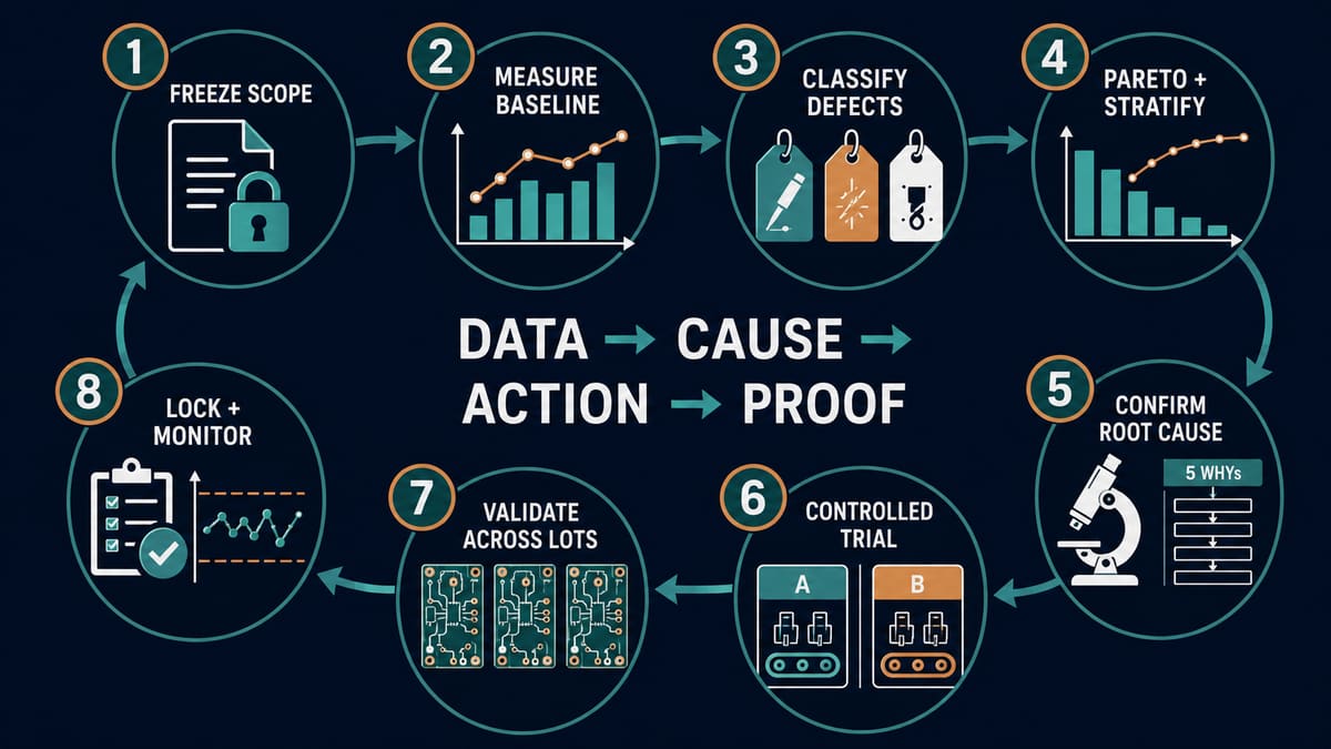
1. Freeze product and process scope. Select one assembly revision, line, shift, period and test boundary. Mixing revisions makes the baseline meaningless.
2. Build a clean baseline. Record units in, units passing first time, defects by station, rework and escapes. Keep “no fault found” separate from confirmed defects.
3. Create a defect taxonomy. Use observable categories such as insufficient paste, bridge, missing part, wrong polarity, placement offset, open joint, void, programming or functional failure. Avoid vague labels like “bad soldering.”
4. Pareto by occurrence and consequence. Rank defect families, then stratify by package, reference, stencil aperture, feeder, machine, shift, material lot and time. The most frequent issue is not always the costliest or riskiest.
5. Separate source families. Decide whether evidence points to design/DFM, incoming PCB, component/BOM, printing, placement, reflow, THT, handling or test. Repeated repair without source classification does not improve the process.
6. Confirm the mechanism. Use overlays, microscope/X-ray, profile data, SPI trends, feeder logs, continuity or controlled swaps. A plausible story is not yet root cause.
7. Define one controlled countermeasure. Change the stencil, support fixture, program, feeder, profile, work instruction, design or test only after the mechanism is supported. Record the old and new state.
8. Run a confirmation trial. Use the same product and clear acceptance criteria. Watch for transferred defects: reducing bridging by reducing paste can create opens.
9. Validate over time and lots. Confirm the change survives normal material, operator and equipment variation. A single good board proves little.
10. Lock and monitor. Update controlled files, programs, training, inspection limits and change records. Set a reaction plan for drift.
Why Should Improvement Start Before Solder Paste Printing?
Many line defects originate in design data or materials. Check land patterns, component spacing, thermal balance, fiducials, panel support, test access, BOM specificity and CPL orientation before tuning machines. A wrong footprint can repeatedly pass placement programming and still fail assembly.
How Can Solder Paste Printing Be Stabilized?
Use SPI or defined visual measurements to connect deposit results to stencil design, cleanliness, support, paste condition and printer settings. Investigate trends by aperture and location rather than changing pressure or speed globally.
| Print signal | Check first | Avoid |
| Low volume at same apertures | Clogging, release geometry, underside contamination | Increasing pressure everywhere |
| Offset across whole board | Fiducial alignment, board support, clamping | Editing individual apertures |
| Bridging after print | Board-to-stencil gap, smear, aperture/foil choice | Blaming reflow before inspecting print |
| Progressive degradation | Cleaning interval, paste condition, stencil underside | Using only end-of-shift yield |
How Do Placement and Reflow Data Close the Loop?
Placement logs, AOI offsets and reflow profiles should be linked to the same board revision and time window. Repeated offset on one reference may indicate footprint, pickup or pad-geometry issues; a line-wide trend suggests calibration, fiducial or program problems.
Measure the profile on the actual loaded board at representative thermal locations. Oven setpoints are inputs, not evidence of component temperature. Follow solder-paste and component guidance; do not use universal peak or dwell values.
How Should AOI, X-Ray and Electrical Tests Be Used?
Use each test for the defect it can observe, then feed confirmed results upstream. AOI can find visible placement and joint anomalies; X-ray reveals hidden structures; ICT/flying probe finds connectivity and component faults; functional test confirms defined behavior. None replaces the others automatically.
| Finding | Best upstream feedback | Evidence needed |
| AOI polarity error | CPL/library/program and first-article check | Drawing, package marking and program revision |
| X-ray hidden open | Paste, placement, pad/thermal and profile review | SPI/profile/X-ray correlation |
| ICT open on random leads | Joint inspection stratified by reference/lot | Failure analysis, not repeated resolder only |
| Functional intermittent | Test fixture, connector, joint and software boundary | Reproducible failure and controlled A/B test |
How Do You Distinguish Design Problems from Process Problems?
A defect tied to one reference across machines and lots often points toward design or package interaction; a defect moving with a feeder, line, stencil, shift or material lot points toward process or material. This is a starting hypothesis, not a verdict. Confirm with a controlled swap or measurement.
What Should Be Reviewed at the First Article?
- PCB, BOM, CPL, program and drawing revisions agree.
- Substitutions and component markings are approved.
- Stencil exceptions and first-print evidence are reviewed.
- Critical placement, polarity and mechanical interfaces are checked.
- Actual reflow profile is approved for the assembly.
- AOI/X-ray scope matches package risk.
- Programming and functional fixtures use controlled versions.
- Defects, concessions and actions are recorded before release.
How Do You Prevent a Prototype Process from Failing at Volume?
Prototype success may depend on expert attention, manual touch-up and favorable material. Before volume, document programs, tooling, inspection limits, changeover checks, maintenance, training and reaction plans. Run pilot production under normal operators and traceable lots instead of extrapolating from one hand-built unit.
How Should You Evaluate an Assembly Supplier’s Improvement System?
Ask for the logic and evidence, not an unsupported yield percentage. A capable supplier can define its metrics, show how defect data is stratified, explain root-cause confirmation, control revisions and demonstrate that corrective actions are monitored after closure.
Frequently Asked Questions
What is the first step in improving PCB assembly yield?
Freeze the product, station and metric definition, then collect a trustworthy baseline. Do not tune equipment before knowing where defects first appear.
Is first-pass yield the same as final yield?
No. Final yield may include repaired units; first-pass yield excludes repair at the defined checkpoint.
Does adding AOI automatically improve quality?
No. Inspection finds certain defects. Improvement requires confirmed findings to change an upstream design, material or process control.
Why are solder defects random?
They may only appear random because data is not stratified by reference, aperture, feeder, lot, shift or time. Segment the evidence before choosing a cause.
Should every defect be reworked?
Follow product acceptance and rework rules. Some products or defects require scrap, concession or engineering review; repeated repair can also hide systemic causes.
How many boards prove an improvement?
There is no universal count. Use risk, normal process variation and an agreed statistical/quality plan rather than one successful sample.
What files help a supplier improve assembly?
Provide Gerbers/ODB++, BOM, CPL, drawings, approved substitutions, test specifications, revision history and defect examples.
How do I know a corrective action is closed?
The mechanism is verified, the change passes confirmation, controlled documents are updated and monitoring shows the defect does not recur under normal variation.
Request a PCB Assembly Improvement Review
Send PCBTRY your current release package, quantities, process route, defect Pareto, inspection images and test failures. We can review DFM, sourcing, stencil, placement, thermal, inspection and test handoffs before proposing a controlled production or quotation plan.



0 Comments