Blog
Ceramic PCB Manufacturing Process: Substrates, Metallization and Testing
See how ceramic PCB substrate, metallization route, circuit formation, profiling, inspection and reliability testing are selected and controlled.



See how ceramic PCB substrate, metallization route, circuit formation, profiling, inspection and reliability testing are selected and controlled.
Build a ceramic PCB testing process that matches substrate, metallization, assembly and application risks, with evidence, records and escalation points.
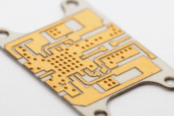
A Ceramic PCB, as the name suggests, is a printed circuit board that uses ceramic material as the substrate. Unlike traditional PCBs that use organic resins (like FR-4) as the base material, ceramic PCBs are sintered from inorganic ceramic materials such as Alumina (Al₂O₃), Aluminum Nitride (AlN), and Beryllium Oxide Read more
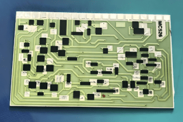
What Is Ceramic PCB? A ceramic PCB is a circuit board that uses ceramic materials as its base instead of traditional FR4. These materials include alumina, aluminum nitride, and others. The ceramic base provides excellent thermal conductivity, high insulation, and strong mechanical strength. Ceramic PCBs are often used in industries Read more
If you have any enquiry about quotation or cooperation, please feel free to email us at [email protected] or use the following enquiry form. Oursales representative will contact you within 24 hours. Thank you for your interest in our products.