




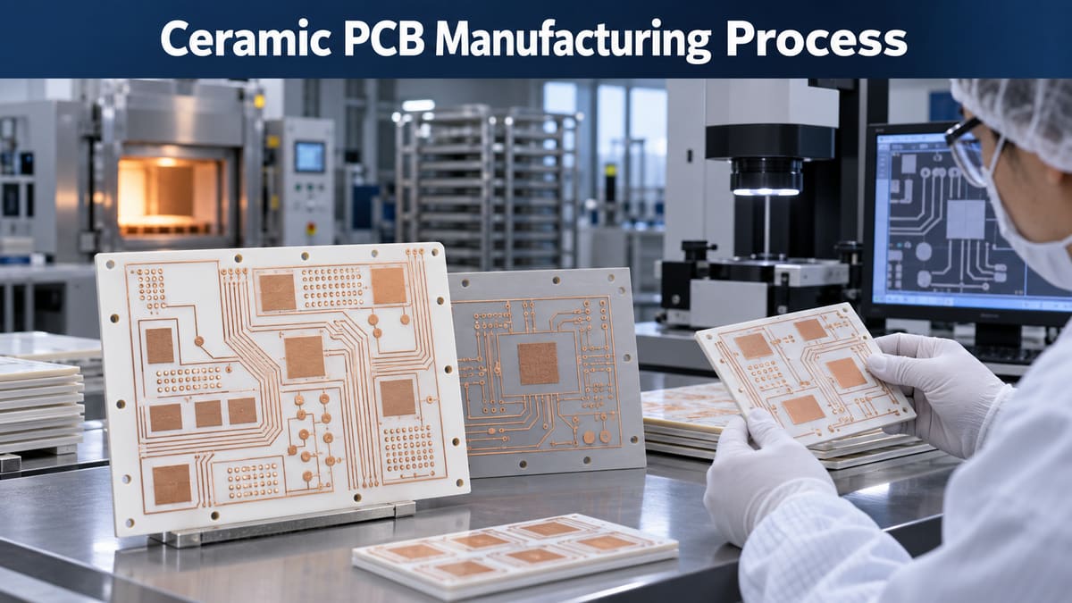
The ceramic PCB manufacturing process forms conductive circuits on alumina, aluminum nitride, silicon nitride, or another engineered ceramic instead of an organic laminate. Designers use ceramic substrates when thermal transfer, electrical insulation, dimensional stability, or operation near heat sources outweigh the cost and mechanical tolerance of conventional FR-4. Common applications include power modules, high-power LEDs, RF packages, sensors, and compact hybrids.
The first manufacturing decision is not “which step comes next?” but “which ceramic and metallization route fits the product?” pcbtry supports ceramic PCB engineering review, fabrication coordination, inspection, and assembly planning. Send Gerber data, drawings, substrate and copper requirements, stack-up, finish, quantity, and acceptance tests for a manufacturability review and quotation.
What Is a Ceramic PCB Manufacturing Process?
A ceramic PCB manufacturing process is a drawing-controlled method for joining and patterning conductive material on a ceramic dielectric, then finishing, profiling, and testing the circuit. The route may start with a fully fired ceramic tile that receives copper or printed metal, or with unfired ceramic tapes whose vias and conductors are built into a multilayer structure before co-firing.
That distinction prevents a common specification error. DBC, DPC, AMB, thick film, and thin film are not interchangeable labels, while LTCC and HTCC are co-fired multilayer systems rather than ordinary copper-clad boards. A quote that says only “ceramic PCB” leaves the manufacturer guessing about conductor thickness, feature resolution, thermal path, joining method, and reliability target. For a basic material comparison before process selection, see ceramic PCB versus FR-4.
How Does the Ceramic PCB Manufacturing Process Work?
The general workflow below applies to most projects, but the circuit-formation stage branches by technology. A reliable traveler identifies the selected route instead of forcing every ceramic design through one generic sequence.
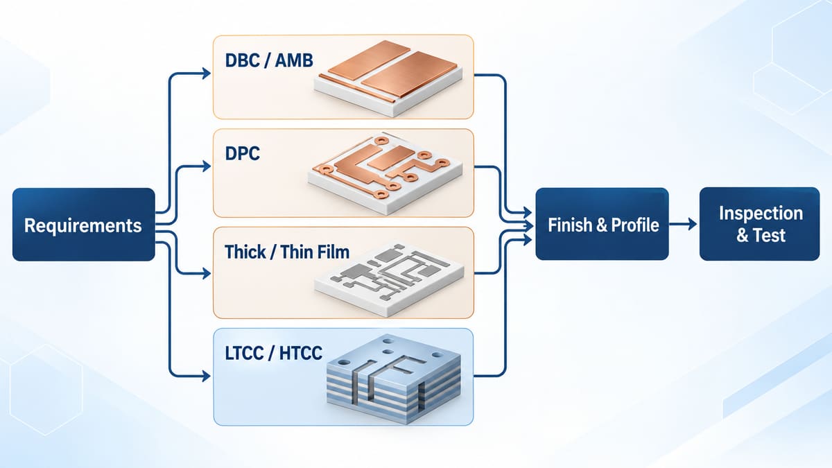
1. Engineering review and process-route selection. CAM and process engineers reconcile Gerber or ODB++ data, drawings, layer order, substrate grade and thickness, conductor construction, hole and edge details, finish, flatness, tolerances, assembly method, and test requirements. They then choose a feasible route: for example, bonded copper for a power circuit, plated copper for finer geometry, printed film for functional pastes, or co-fired ceramic for embedded multilayer interconnects. An unresolved conflict is returned as a question; silently choosing a route can change current capacity, pad geometry, and reliability.
2. Ceramic substrate or green-tape preparation. Fired-substrate routes begin with ceramic sheets inspected for identity, thickness, flatness, surface condition, chips, and cracks, followed by cleaning and any required lapping or activation. LTCC and HTCC instead begin with unfired tape that is cut and conditioned for layer processing. Contamination can weaken metallization adhesion, while a chipped edge can propagate a crack during later handling or thermal loading.
3. Holes, vias, cavities, and alignment features. The method depends on material condition and route. Green ceramic layers may be punched or laser structured before via filling; fired ceramic may require qualified laser or mechanical processing. The drawing must distinguish electrically connected vias, mounting holes, cavities, and edge features. Heat input, debris, taper, positional error, or microcracking can create a weak interconnect or fracture origin even when the opening looks dimensionally acceptable from one side.
4. Circuit metallization and pattern formation. This is where routes diverge. DBC bonds copper foil to ceramic and then images and etches the circuit. AMB uses an active-metal brazing system to join copper to a compatible ceramic. DPC establishes an adhesion/seed system, images the circuit, builds copper by plating, and removes unwanted seed material. Thick film screen-prints conductor or functional paste and fires it; thin film deposits a much thinner metal system and uses photolithographic patterning. LTCC/HTCC print conductors and fill vias on green layers before stacking. The engineer controls surface preparation, registration, film thickness, sidewall/profile, adhesion, and route-specific thermal cycle. Drift can cause opens, bridges, undercut, weak pads, or conductor lift.
5. Lamination and firing where the route requires them. LTCC/HTCC layers are aligned, stacked, laminated, binder-burned out, and co-fired under a qualified profile. Thick-film pastes also require a specified firing cycle, but a DPC circuit does not become LTCC simply because heat is used somewhere in production. Shrinkage compensation, atmosphere, pressure, temperature profile, and material compatibility must be controlled. Registration loss, trapped contamination, incomplete densification, warpage, blistering, or conductor interaction may otherwise be locked into the structure.
6. Plating, surface finish, and protective layers. Route and assembly method determine whether additional copper build, nickel/gold systems, silver, solder mask, passivation, or another finish is appropriate. The finish drawing should state which pads are for soldering, wire bonding, brazing, probing, or exposed conduction. A finish selected only by name can fail if its thickness, underlying metal, cleanliness, or bonding compatibility is not defined.
7. Profiling, cleaning, and handling. Laser cutting, dicing, sawing, or another qualified method separates parts and creates the finished outline. Ceramic is hard but brittle: poor support, excessive local heat, or an aggressive edge condition can produce chips or microcracks. Cleaning must remove process residue without attacking metal or trapping contamination in holes and cavities. Finished pieces need controlled trays or fixtures rather than loose-board handling.
8. Inspection, electrical test, and release. Visual inspection and dimensional measurement check the substrate, pattern, holes, edges, and finish; AOI can compare circuit geometry; electrical testing verifies continuity and isolation against released data. Depending on the design and acceptance plan, cross-sections, adhesion evaluation, X-ray, flatness measurement, wire-bond or solderability checks, thermal cycling, or other qualification tests may be required. A certificate without the agreed test method and acceptance criteria does not prove that the product interface is fit for use.
Which Ceramic Material and Metallization Route Should You Choose?
Choose the material and conductor route together. Thermal demand alone does not decide the stack: mechanical loading, copper mass, circuit resolution, dielectric behavior, joining process, environment, availability, and cost all constrain the answer. Exact properties must come from the approved grade datasheet, not a generic material name.
| Option | Best fit | Manufacturing trade-off | What to confirm |
|---|---|---|---|
| Alumina | Cost-sensitive hybrids, LEDs, sensors, general insulation | Widely used, but thermal performance and strength depend on grade and construction | Purity/grade, thickness, surface condition, metallization compatibility |
| Aluminum nitride | Thermally demanding power and optoelectronic designs | Better heat spreading can justify higher material and processing cost; handling and finish still matter | Grade datasheet, thermal path, moisture/cleaning controls, copper interface |
| Silicon nitride | Power modules needing a demanding thermal-mechanical balance | Route and supply base are more specialized | Strength/reliability target, AMB or other qualified joining system, availability |
| DBC | Thick copper and power paths | Bonded foil supports power structures but pattern geometry and copper/ceramic stress require review | Copper and ceramic thickness, isolation geometry, edge relief, plating |
| DPC | Finer patterned copper and controlled plated construction | More deposition, imaging, and plating controls; conductor build and adhesion are process-specific | Seed/adhesion system, finished copper, feature rules, via method |
| Thick or thin film | Hybrid circuits, functional resistors/heaters, or fine deposited conductors | Paste or deposited-film system determines geometry and assembly compatibility | Conductor system, firing/deposition route, trimming, bonding/soldering interface |
| LTCC or HTCC | Multilayer ceramic packages with internal vias and conductors | Shrinkage, layer registration, conductor compatibility, and co-fire profile are coupled | Material system, layer design rules, via fill, cavities, post-fire finish |
Do not copy a nominal line width, copper thickness, or thermal value from another supplier’s marketing table into the drawing. Ask the selected manufacturer for route-specific design rules and lock the accepted construction into the fabrication specification.
How Should the Stack-Up and Layout Be Designed?
A ceramic stack-up must define the electrical path, thermal path, and mechanical load path at the same time. Start with component footprints and heat sources, then establish conductor layers, dielectric thickness, vias, backside metal, isolation distances, cavities, and attachment interfaces. In co-fired multilayers, every internal layer and via must also survive registration and shrinkage; in DBC/AMB structures, copper balance and edge geometry influence stress.
- State substrate material by grade or approved equivalent, not only “ceramic.”
- Define finished metal construction and acceptable finish by functional area.
- Identify solder, braze, wire-bond, pressure-contact, and thermal-interface surfaces.
- Keep critical copper edges, holes, and singulation features compatible with the supplier’s route.
- Provide flatness and profile requirements only where the assembly truly needs them.
- Ask for thermal and mechanical review where large copper areas or concentrated heat loads create stress.
What Manufacturing Challenges Cause Ceramic PCB Failures?
The most serious failures occur at interfaces: metal to ceramic, via to conductor, layer to layer, finish to assembly, and finished edge to mechanical fixture. Ceramic does not yield like an organic laminate, so local stress and handling damage deserve explicit controls.
| Risk | What creates it | Evidence to request |
|---|---|---|
| Weak metallization adhesion | Contamination, poor surface preparation, incompatible metal system, process drift | Route record, adhesion acceptance method, representative cross-section where applicable |
| Cracks or edge chips | Laser/dicing damage, unsupported handling, sharp geometry, assembly clamping | Edge inspection criteria, magnified inspection, packaging method |
| Copper/ceramic stress | Unbalanced metal, thick copper, thermal cycling, CTE mismatch | Construction review, thermal-cycle qualification tied to the application |
| Open or resistive vias | Incomplete fill/plating, debris, misregistration, firing interaction | Electrical test, X-ray or section evidence when specified |
| Pattern or isolation defect | Imaging, printing, etching, plating, or registration variation | AOI and dimensional results against released data |
| Assembly-interface failure | Wrong finish, poor cleanliness, unsuitable pad geometry, uncontrolled heating | Finish certificate plus solderability/wire-bond evidence required by the drawing |
How Does Design Affect Reliability?
Reliability is not added by final inspection; it is designed into geometry and interfaces before tooling. Large uninterrupted copper regions, abrupt copper-density changes, holes near stressed edges, tight internal registration, and unsupported ceramic spans can turn normal thermal or assembly loads into concentrated stress. The manufacturer should review the layout with the actual material pair and metal thickness, not only run a generic Gerber check.
Use application-relevant acceptance tests. A board that passes continuity may still be unsuitable for wire bonding, power cycling, repeated temperature change, or a clamped module. Conversely, demanding every available test raises cost without necessarily reducing the real risk. Link each test to a failure mode and a stated acceptance criterion. A structured DFM and DFA review should therefore include both bare-substrate and downstream assembly interfaces.
What Tests Ensure Ceramic PCB Quality?
The minimum release package normally combines identity, dimensions, visual condition, circuit geometry, and electrical results. Reliability-sensitive projects add tests based on the use environment and joining method.
- Incoming/substrate inspection: grade traceability, thickness, flatness, surface condition, cracks, and chips.
- In-process inspection: registration, printed/deposited pattern, plating or film build, via condition, and firing/profile records.
- Final dimensional and visual inspection: outline, holes, conductor features, edge quality, finish, markings, and cleanliness.
- Electrical test: continuity and isolation against a released netlist or test data.
- Interface verification: adhesion, solderability, wire-bondability, or brazing checks where the product requires them.
- Reliability qualification: cross-section, thermal cycling, power cycling, X-ray, hermeticity, or other tests only when defined by the application and acceptance plan.
Before production, agree on sample size, test method, acceptance boundary, report format, and action for a failure. “Tested” is not a complete purchase requirement.
How Long Does Ceramic PCB Manufacturing Take?
Lead time depends more on route maturity and material availability than on a universal prototype-versus-production label. Standard fired substrates and an established pattern route may move faster than a custom ceramic grade, new co-fired stack, unusual finish, laser cavity, or application-specific reliability qualification.
For prototypes, allow time for DFM questions, route confirmation, tooling/program preparation, and first-article evidence. For repeat production, stable released data and approved materials reduce engineering churn, but batch firing, plating, profiling, and qualification still follow controlled queues. Ask the supplier to separate engineering review, material procurement, fabrication, qualification, and shipping in the schedule rather than accepting one unexplained date.
How Do You Choose a Reliable Ceramic PCB Manufacturer?
Choose the supplier that can explain why its proposed route matches your design and can show how the critical interfaces will be controlled. A broad “ceramic PCB capability” claim is less useful than a route-specific DFM response.
- Ask which ceramic grades and metallization routes are actually produced or qualified.
- Request route-specific design rules for metal thickness, features, vias, edges, and flatness.
- Confirm how material identity, firing/plating records, and finished parts are traceable.
- Ask which inspection and reliability tests are in-house, outsourced, or unavailable.
- Define how cracks, chips, adhesion, electrical defects, and finish nonconformities are accepted.
- Review packaging and handling for brittle parts.
- Send the complete release package and compare the engineering questions—not only unit price.
For a route-specific capability discussion and quotation path, review the ceramic PCB manufacturing service.
What Files and Specifications Are Needed for a Quote?
Send a package that lets engineering reproduce both the circuit and its functional interfaces:
- Gerber or ODB++ circuit data and NC drill/laser data;
- dimensioned fabrication drawing with datum scheme and profile;
- substrate material, grade, thickness, and approved alternatives;
- metallization route if fixed, plus finished conductor and finish requirements;
- layer stack, via/cavity details, and controlled electrical requirements;
- assembly method and functional areas for soldering, brazing, or wire bonding;
- inspection, test, qualification, documentation, and traceability requirements;
- prototype and production quantities, packaging, and delivery destination.
Frequently Asked Questions
Is every ceramic PCB made by firing copper onto ceramic?
No. Thick-film and co-fired systems use firing, while DBC, AMB, DPC, and thin-film routes create the metal-to-ceramic system differently. The drawing and supplier proposal should name the selected route.
What is the difference between DBC and DPC?
DBC bonds copper foil to ceramic before patterning; DPC creates an adhesion/seed system and builds patterned copper by plating. Neither is automatically better—the decision depends on copper construction, geometry, substrate, thermal-mechanical demand, and supplier process.
Are LTCC and HTCC types of ordinary ceramic PCB?
They are co-fired multilayer ceramic technologies. Conductors and vias are formed on green ceramic layers, which are stacked, laminated, and fired into a monolithic structure.
Which ceramic substrate is best for heat dissipation?
Aluminum nitride is often evaluated for demanding thermal paths, but “best” depends on the exact grade, thickness, interface, copper system, mechanical load, availability, and cost. Use approved datasheets and a complete thermal model.
What commonly causes ceramic PCB cracking?
Edge damage, poor handling, local mechanical constraint, aggressive profiling, abrupt geometry, and thermal-mechanical stress can initiate or propagate cracks. Specify inspection criteria and review the assembly fixture as well as fabrication.
Can ceramic PCBs use plated through-holes?
Some routes support metallized holes or filled vias, but the method and design limits differ between fired substrates and co-fired structures. Provide hole function and reliability requirements so the supplier can confirm a qualified route.
What tests should be required?
Begin with dimensional, visual, and electrical acceptance. Add adhesion, cross-section, X-ray, solderability, wire-bond, thermal cycling, power cycling, or hermetic tests only when they address a defined failure mode.
Why can two ceramic PCB quotations differ greatly?
They may assume different ceramic grades, metallization routes, metal thicknesses, finishes, tolerances, yield risks, test plans, or documentation. Normalize the technical scope before comparing price.
Request a Ceramic PCB Engineering Review
A useful quote should confirm the substrate, metallization route, construction, inspection plan, and unresolved design risks. Send your Gerber or ODB++ package, fabrication drawing, substrate and conductor specifications, assembly method, quantities, and acceptance tests to [email protected]. The engineering review can then identify route conflicts before tooling and provide a quote based on the released requirements.



0 Comments