




Define the Ceramic PCB You Are Actually Testing
A ceramic PCB test plan starts by identifying the item under test. “Ceramic PCB” can describe an alumina or aluminum-nitride substrate, a DBC or AMB power substrate, a DPC circuit, an LTCC assembly, or a populated ceramic-board assembly. These constructions do not share one universal test sequence or one set of acceptance limits. Record the substrate material and thickness, metallization system and thickness, layer construction, finish, assembly state, intended environment, drawing revision, and the requirement that owns acceptance.
That definition prevents an avoidable mistake: treating a visual check, an electrical screen, or a thermal-cycle result as proof that the entire board is qualified. A board can have correct continuity yet still need a separate assessment of substrate cracking, copper-to-ceramic integrity, solder joints, dielectric clearance, or application-level thermal behavior.
Start With the Requirement, Not a Generic Test List
Before selecting equipment, translate the product requirement into questions that a test can answer. For example, a customer drawing may require conductor geometry and isolation verification; a power-module design may need evidence about heat flow and cycling robustness; an assembly requirement may need solder-joint inspection and functional verification. The governing drawing, material data sheet, purchase specification, customer test plan, and applicable standard define the method, sample, condition, acceptance criterion, and disposition path.
If any of those inputs are missing, do not invent a pass limit. Mark the result as a screening observation and escalate the missing requirement. This is especially important for high voltage, high power, safety-related, hermetic, aerospace, medical, or destructive testing.
Build a Ceramic PCB Test Plan by Stage
A practical plan separates evidence by production stage. Incoming inspection asks whether the delivered substrate and documentation match the order. Fabrication inspection asks whether dimensions, pattern, metallization and visible workmanship match the controlled definition. Finished-board electrical test screens connectivity and isolation according to the approved test condition. Assembly inspection addresses component placement, solder attachment and rework risk. Qualification or application validation then evaluates the combined board under the defined use condition.
For each stage, name the sample population, method, instrument or fixture, condition, acceptance owner, record format and escalation route. A result without its test condition is difficult to compare later, particularly where temperature, humidity, bias, fixture pressure, probe location or board state changes the reading.
Decision Table: Match the Risk to the Evidence
| Observed risk or question | Useful evidence category | Record before deciding | Do not claim |
|---|---|---|---|
| Chip, edge or surface damage | Controlled visual inspection; microsection only when authorized | Board ID, magnification, location, drawing reference and images | That an intact-looking surface proves internal integrity |
| Open, short or wrong net | Approved continuity, resistance or net test | Test points, board state, fixture, range, criterion and result | That connectivity alone proves insulation or reliability |
| Isolation concern | Requirement-defined insulation or withstand test | Voltage, duration, environment, safety controls and criterion | A universal test voltage or pass value |
| Metallization or attachment concern | Applicable adhesion, bond, solderability or assembly inspection | Construction, method, sample and disposition rule | That substrate testing covers assembly integrity |
| Thermal-cycle concern | Controlled cycling plus requirement-relevant performance measurement | Temperature profile, dwell, cycle count, sample and pre/post evidence | That cycle count directly predicts service life |
| Field or system behavior | Application-level functional and thermal validation | Load, ambient, interfaces, measurement locations and limits | That a coupon or bare-board result proves system performance |
Incoming and Fabrication Inspection
Begin with identity and traceability: purchase order, material designation, lot information, drawing revision and supplier documentation. Then inspect the board against the approved definition. Depending on the construction and requirement, this can include dimensions, edge condition, holes or features, conductor pattern, registration, surface condition, finish, visible cracking, chips, void indications and contamination. IPC’s TM-650 listing includes a ceramic-substrate microsection method, but destructive analysis should be planned and authorized rather than used as a routine substitute for controlled process evidence.
Use consistent lighting, magnification, handling controls and an agreed defect vocabulary. A photograph is most useful when it includes the board identifier, location reference and inspection condition. If the drawing does not define an allowable condition, record the observation and request a disposition instead of assigning your own acceptance limit.
Electrical Verification: Opens, Shorts and Insulation Boundaries
Electrical testing should answer a specific question. A continuity or resistance check can screen intended conductive paths; an approved net test can look for opens and shorts; an insulation or withstand test may be needed where the requirement defines the voltage, duration, environment, guards and safety controls. Test points must be tied to the netlist, drawing or fixture program, not guessed from appearance.
Record board state and test conditions. A populated board can show parallel paths, semiconductor junction behavior, stored energy or fixture effects that change a reading. Treat an unexpected in-circuit result as a clue until it is compared with the design, a known-good reference, or a justified isolation step. Do not apply high voltage merely because a board is ceramic; the requirement and safe procedure determine whether that test is appropriate.
For the basic measurement discipline behind these checks, see PCBtry’s guides on how to test a PCB and how to troubleshoot a PCB. They support the measurement workflow, while this article keeps the ceramic-substrate and qualification boundaries in view.
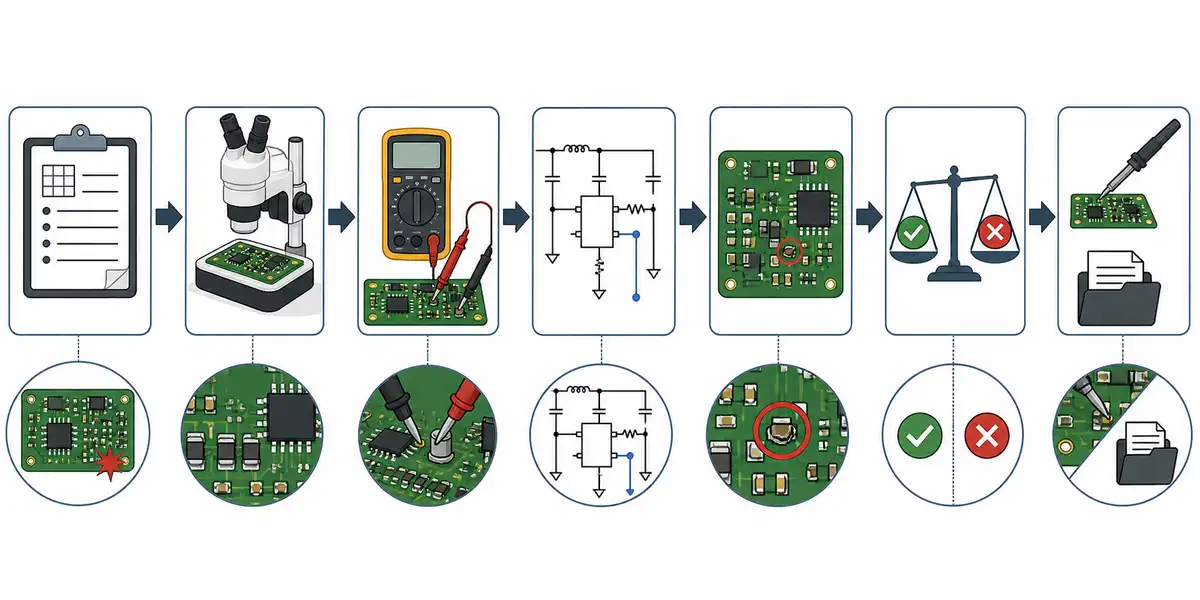
Why this image is here: It provides a compact order for deciding whether to inspect, measure, document or escalate. Without that sequence, a reader may treat a convenient measurement as a complete qualification result.
Metallization, Bond and Assembly Checks
The ceramic body, metallization and mounted assembly are related but different verification targets. A metallized ceramic substrate may need evidence related to conductor pattern, bond interface or surface condition. A populated assembly may additionally need placement, polarity, solder-joint, void, rework or functional evidence. Select the method from the actual construction and applicable requirement; a method suitable for one DBC, DPC, thick-film or LTCC construction is not automatically transferable to another.
For rework or destructive evaluation, preserve traceability and define the question first. Removal can alter a part, pad or substrate, so a post-rework observation may not reveal the original failure mechanism. When a defect is suspected, record the original condition before any authorized intervention.
When the outcome shows that the design needs controlled fabrication review rather than more bench screening, PCBtry’s PCB manufacturing guides provide a useful next step for preparing the production discussion.
Thermal and Environmental Reliability: What a Result Can and Cannot Prove
Thermal cycling is commonly used to compare the reliability of metallized ceramic substrates because temperature changes create stress between materials. Rogers notes that thermal cycling is an accelerated comparison method, not a direct prediction of real application lifetime. The critical interpretation therefore depends on the construction, test profile, sample set and the performance measure that matters to the application.
Visual inspection after cycling can find obvious damage, but visual evidence may not be enough to decide whether a defect is functionally critical. Where heat transfer is the requirement, combine the exposure with a requirement-relevant thermal performance measurement. Where electrical isolation, bond integrity or function is the concern, select the corresponding approved post-test evidence. Do not reuse another supplier’s cycle count, temperature range or result as your board’s acceptance criterion.
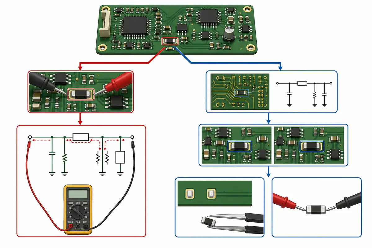
Why this image is here: It distinguishes a preliminary observation from confirmation. Removing it would make the article’s central evidence boundary easier to miss during test planning.
Case Study: Compare Ceramic Substrates Under Stated Conditions
Problem
A power-substrate team needs evidence to compare thermal-cycle robustness of metallized ceramic material combinations under a defined reference layout and test condition.
Treatment
Use a controlled thermal-cycle comparison on the reference layout, then select the ceramic and copper material combination whose published result meets the project requirement. Do not use a visual observation or generic cycle count alone.
Action Taken
Rogers tested its reference layout under stated cycling conditions and compared Endurance DBC combinations with alternative metallized ceramic substrate combinations.
Result
The product information reports improved cycling reliability for the listed Endurance combinations under its stated reference-layout conditions. Results remain layout- and condition-dependent. This is published external substrate-test evidence, not a PCBtry test result and not a universal ceramic-PCB acceptance limit.
| Case element | Published interpretation |
|---|---|
| Background | Published reference-layout comparison of metallized ceramic substrate combinations. |
| Problem | The team needs requirement-relevant evidence for thermal-cycle material selection. |
| Treatment | Run a controlled comparison and select the material combination against the project requirement. |
| Action taken | Rogers compared listed material combinations under stated reference-layout cycling conditions. |
| Result boundary | Published improvement is condition-dependent and is not a universal ceramic PCB pass limit. |
Create a Traceable Test Record
A useful record allows another engineer to reproduce the decision. Include the board and sample identity, drawing and revision, material and construction, test objective, method or work instruction, equipment and calibration status where applicable, fixture, settings, environmental condition, operator, date, raw result, criterion, disposition, photos or files, and escalation reference. Record deviations rather than silently normalizing them.
Keep a separate status for screening, acceptance, qualification and investigation. This prevents a passed continuity screen from being reported as a qualified reliability result. For a buyer, the same separation makes it easier to request the evidence that supports a supplier’s claim without asking for irrelevant test data.
Ceramic PCB Testing Checklist
Saveable checklist: This visible 12-point checklist is a general planning aid. You may copy or print it for a project file. It is not a laboratory report, certificate, manufacturing approval or proof that a particular ceramic PCB passed.
- Identify substrate material, construction, finish and assembly state.
- Freeze the drawing, revision and acceptance owner.
- State the product risk or failure question.
- Separate incoming, fabrication, assembly and application evidence.
- Select only methods supported by the applicable requirement.
- Define the sample population and traceability path.
- Record equipment, fixture and test condition.
- Set safety controls before high-voltage, thermal or destructive work.
- Record raw observations before repair or rework.
- Compare results with the approved criterion, not a generic web value.
- Label the outcome as screening, acceptance, qualification or investigation.
- Escalate missing criteria, safety uncertainty or conflicting evidence.
FAQs About Ceramic PCB Testing
What is included in a ceramic PCB testing process?
A process can include requirement review, incoming inspection, fabrication checks, electrical verification, assembly inspection, reliability evaluation and application validation. The actual selection depends on the board construction and requirement.
Is ceramic PCB testing different from FR-4 PCB testing?
Some electrical and workmanship checks overlap, but ceramic substrate, metallization and assembly behavior can require different methods, fixtures and acceptance criteria. Do not transfer a limit without confirming applicability.
Do ceramic PCBs always need thermal cycling?
No. Use thermal cycling when the requirement, risk analysis or qualification plan calls for it. It is not a universal production screen.
Can visual inspection prove a ceramic PCB is reliable?
No. It can find visible conditions, but internal integrity and functional criticality may require other evidence defined by the test plan.
Which electrical tests are used for ceramic PCBs?
Continuity, resistance, opens/shorts and insulation-related tests may be used when the design and requirement define the method, condition and acceptance criterion.
What should be recorded during ceramic PCB testing?
Record board identity, revision, construction, method, equipment, fixture, conditions, raw results, criterion, disposition and any deviation or escalation.
Can I use a generic hipot voltage for a ceramic PCB?
No. Test voltage and duration must come from the applicable requirement and safe procedure. Ceramic material alone does not define a safe or valid test setting.
Does a passed continuity test prove insulation performance?
No. Continuity checks conductive paths. Insulation performance requires its own requirement-defined evidence.
How do I test metallization on a ceramic PCB?
First identify the process route and requirement. Pattern inspection, surface review, bond or adhesion evidence and assembly checks may be relevant, but the method must match the actual construction.
What should a buyer request from a ceramic PCB supplier?
Request the material and construction definition, drawing revision, relevant inspection or test evidence, test conditions, acceptance basis, traceability and any open deviation or limitation.
Sources
- IPC TM-650 Test Methods Manual
- Rogers: Reliability of Metallized Ceramic Substrates for Power Electronics Applications
- Rogers: curamik Endurance Product Information
- Fluke: Continuity Testing with a Multimeter
- Texas Instruments: Board-Level Troubleshooting
Need a ceramic PCB test plan that matches your drawing and application? Share the substrate, metallization, assembly state, environment and required evidence with PCBtry so the manufacturing and verification discussion starts with the right constraints.



0 Comments