Blog
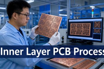
Inner Layer PCB Process: Imaging, Etching and Registration Checks
See how PCB inner layers move from CAM compensation and copper preparation through imaging, etching, AOI, oxide treatment, and lamination release checks.



See how PCB inner layers move from CAM compensation and copper preparation through imaging, etching, AOI, oxide treatment, and lamination release checks.
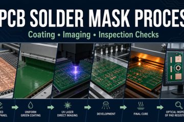
See how PCB solder mask is prepared, coated, imaged, developed, cured and inspected for registration, coverage and adhesion defects.
If you have any enquiry about quotation or cooperation, please feel free to email us at [email protected] or use the following enquiry form. Oursales representative will contact you within 24 hours. Thank you for your interest in our products.