




The inner layer PCB process converts copper-clad cores into the buried circuit layers of a multilayer board. CAM preparation, copper cleaning, photoresist imaging, development, etching, resist stripping, AOI, surface treatment, and registration checks must all be completed before lamination. After pressing, an inner-layer open, short, misregistration, or contamination defect is normally inaccessible, so the strongest quality controls occur while each core can still be inspected.
This process is used whenever a PCB needs internal signal, power, or ground layers. Compared with an outer layer, an inner layer has no later solder-mask or surface-finish correction opportunity; its geometry and bond surface become embedded in the stack. PCBtry can review Gerber/ODB++ data, stackup drawings, impedance requirements, and fabrication notes before quotation. Submit the controlled revision through the contact page for an engineering review.

What Is the Inner Layer PCB Process?
The inner layer process is the print-and-etch sequence used to form copper circuitry on the cores inside a multilayer PCB. Each core commonly carries circuitry on both faces, and the approved cores are later combined with prepreg and outer copper during lamination.
Its difficulty comes from cumulative error. Artwork scale, core movement, imaging registration, etch behavior, copper distribution, and lamination movement all affect where a buried pad or plane ends up relative to a drilled hole. A trace that looks acceptable in isolation may still create insufficient annular connection after the stack is pressed and drilled.
How Does the Inner Layer PCB Process Work?
The process follows one controlled route from customer data to lamination-ready cores. The exact equipment and chemistry vary by factory and material system, but the control logic remains consistent.
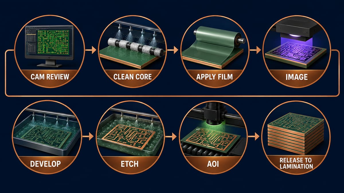
1. CAM Review and Layer Compensation
CAM engineers identify layer polarity, stack position, net relationships, panel tooling, coupons, and manufacturability conflicts. They apply validated scale compensation where required because laminate dimensions can shift during later thermal and mechanical processing. Wrong polarity can turn clearances into copper; wrong scaling can move buried pads away from the drill target.
2. Core Material Issue and Traceability
The factory issues copper-clad cores that match the approved material, dielectric thickness, and copper specification. Lot and orientation control matter because mixing cores or reversing an asymmetric layer pair can change impedance, copper balance, or connectivity. The traveler should tie each core to the job and stack position.
3. Copper Surface Preparation
The copper is cleaned and conditioned so dry-film photoresist can adhere uniformly. Oxidation, fingerprints, particles, water breaks, or over-aggressive brushing can produce resist lift, pinholes, scratches, or nonuniform imaging. A clean surface is judged by the qualified preparation process and inspection evidence, not by appearance alone.
4. Dry-Film Lamination
Photosensitive film is laminated over the copper without wrinkles, bubbles, or trapped debris. Temperature, pressure, speed, and panel cleanliness must stay within the qualified window. Poor film contact can create undercut features, missing copper, or shorts after development and etching.
5. Image Registration and Exposure
Laser direct imaging or phototool exposure places the circuit image relative to panel targets. Registration systems align the artwork to tooling features, while exposure energy defines how accurately fine spaces and conductors reproduce. Underexposure can weaken resist; overexposure can close small clearances or change feature edges.
6. Development
Development removes the intended soluble resist and leaves a protective pattern over copper that must remain. Incomplete development leaves residue that blocks etching; excessive development attacks protected features. Operators monitor the qualified chemistry and verify that clear copper areas and resist edges are consistent.
7. Copper Etching and Resist Stripping
Etching removes unprotected copper, then stripping removes the remaining resist to reveal the finished inner circuit. Copper thickness, feature direction, chemistry condition, spray behavior, and conveyor settings affect etch uniformity. Excessive etch narrows traces and annular features; insufficient etch leaves copper bridges or shorts.
8. Automated Optical Inspection
AOI compares the manufactured image with the CAM reference or validated feature model. It detects opens, shorts, nicks, protrusions, pinholes, and spacing anomalies that may be difficult to see consistently by eye. Every flagged location still needs disposition: accept, repair where the controlled process allows, or scrap and remake.
9. Bond-Surface Treatment
Approved inner layers receive an oxide, alternative oxide, or other qualified surface treatment to promote bonding with prepreg. The objective is controlled adhesion without damaging fine copper. Contamination, uneven treatment, or excessive handling can contribute to delamination or conductor damage during lamination and service.
10. Registration and Lamination Release
The factory confirms layer identity, orientation, tooling targets, inspection status, surface condition, and traveler completeness before lay-up. Releasing the wrong revision or inverted core cannot be solved by a good press cycle. Only accepted cores should enter the multilayer book.
Which Materials and Inputs Control the Result?
Inner-layer quality begins with the approved stackup and source data. Material family, core thickness, copper weight, resin system, glass construction, and copper distribution affect imaging, etching, dimensional movement, bonding, impedance, and finished thickness.
| Input | What engineering must define | Risk if ambiguous |
| Layer data | Layer name, polarity, order, net intent, revision | Mirrored, swapped, or wrong-polarity circuits |
| Stackup | Core/prepreg sequence, copper intent, finished thickness | Impedance or thickness mismatch |
| Material | Required performance and acceptable substitutions | Uncontrolled thermal or electrical behavior |
| Drill relationship | Pad, clearance, via structure, backdrill or buried-via needs | Breakout or unintended plane connection |
| Impedance | Target, tolerance, reference layer and coupon requirement | Geometry built against the wrong model |
How Are Imaging and Etching Limits Evaluated?
Manufacturability is evaluated as a feature system, not as one minimum trace number. Copper thickness, trace direction, local density, isolated versus nested features, spacing, annular geometry, and panel position all influence the process result.
A supplier should review the smallest traces and spaces together with copper weight and the surrounding pattern. Plane clearances and thermal features need attention because residual copper can create a short even when most of the panel etches correctly. Ask whether the proposed geometry fits a stable production window rather than merely whether one feature has ever been produced.
Why Is Registration Harder on Multilayer Boards?
Registration must anticipate both the present image position and later material movement. A core can pass its own artwork alignment check yet still shift relative to other layers during lay-up and lamination.
- Asymmetric copper can produce uneven dimensional behavior.
- Different materials or glass constructions can move differently.
- Layer count increases the number of interfaces that must align.
- Fine-pitch vias reduce the available registration margin.
- Sequential lamination creates more than one movement history.
Good registration control uses job-specific CAM targets, qualified material data, tooling strategy, measured process feedback, and post-lamination verification. The buyer should request evidence appropriate to the design rather than a generic “high precision” claim.
What Does Inner-Layer AOI Prove—and What Does It Not Prove?
AOI proves that visible conductor geometry was compared with a reference under the configured inspection rules. It can locate many opens, shorts, nicks, protrusions, and residual-copper defects before lamination.
AOI does not prove material identity, bond strength, final registration to drilled holes, impedance, or electrical continuity of the completed multilayer board. Those require traceability, process controls, coupons or measurements where specified, post-lamination inspection, and final electrical testing.
Which Defects Should Engineers Connect to Process Controls?
| Observed risk | Likely process area | Evidence to review |
| Open or narrowed trace | Resist adhesion, exposure, development, over-etch | AOI image, etch control and defect disposition |
| Copper bridge or short | Incomplete development/etch, artwork or contamination | AOI location and CAM reference |
| Pad breakout after drilling | Compensation, registration, material movement | Targets, coupons, X-ray or section data as applicable |
| Delamination | Surface treatment, contamination, material/press compatibility | Traveler, material traceability and reliability plan |
| Impedance shift | Etched geometry, stackup or dielectric variation | Coupon design and specified measurement report |
How Does PCB Design Affect Inner-Layer Yield and Reliability?
Design determines how much manufacturing margin is available. Tight pad-to-clearance relationships, extreme copper imbalance, isolated fine features, poorly defined plane voids, and mixed material assumptions reduce the stable process window.
Before release, verify that each plane clearance belongs to the correct net, reference planes remain continuous under critical signals, copper is balanced where practical, and via structures match the stackup. Provide an IPC-356 netlist when the workflow supports it so CAM can compare connectivity independently of the artwork.
What Quality Evidence Should Be Available Before Lamination?
A lamination release should show that the correct cores passed the required operations and inspections. The exact record format is factory-specific, but the evidence chain should be traceable.
- Approved CAM revision, layer map, polarity, and stackup.
- Material lot and core identification.
- Process traveler completion for preparation, imaging, development, and etching.
- AOI result and disposition of every reportable anomaly.
- Layer orientation and registration-target verification.
- Bond-surface treatment status and handling control.
- Release authorization for the correct lamination book.
How Should You Review an Inner-Layer Process With a Supplier?
Ask questions that produce project evidence instead of marketing adjectives. The answers should connect your geometry and stackup to the supplier’s controlled route.
| Supplier question | Useful answer should identify |
| How will you compensate this stackup? | Material/process history and job-specific CAM method |
| How are inner layers registered? | Targets, tooling, measurement and feedback loop |
| What does AOI compare? | Reference data, defect types and disposition method |
| How is layer identity protected? | Traveler, barcode or equivalent traceability |
| What validates buried-pad alignment? | Applicable coupon, X-ray, section or process evidence |
| What files must be clarified before CAM release? | Layer map, drill relation, stackup, impedance and notes |
Inner-Layer DFM and RFQ Checklist
- Send one controlled Gerber/ODB++ revision with drill and netlist data.
- Define the layer order, polarity, stackup, finished thickness, and copper requirements.
- Identify impedance nets, reference layers, targets, tolerances, and coupon needs.
- Confirm via types, buried structures, backdrill, slots, and pad relationships.
- Flag the smallest traces, spaces, annular features, and plane clearances.
- State material performance requirements and substitution limits.
- Ask how compensation, registration, AOI, traceability, and lamination release are controlled.
- Resolve CAM questions in writing before authorizing production.
Frequently Asked Questions
Are inner PCB layers made before lamination?
Yes. The copper circuits on inner cores are imaged, etched, stripped, inspected, and surface-treated before the cores are laid up with prepreg and outer copper for lamination.
Why is AOI performed before lamination?
AOI finds conductor defects while the core is still accessible and can be dispositioned or replaced. After lamination, a buried open or short can require scrapping the multilayer panel.
What is inner-layer compensation?
It is a controlled CAM adjustment intended to account for predictable dimensional movement in later processing. The value must come from the supplier’s validated material and process data, not a universal number.
What is the difference between inner- and outer-layer etching?
Inner layers are commonly formed on copper-clad cores before lamination, while outer-layer circuitry is processed after the multilayer structure is pressed and drilled. The detailed plating and etch sequence can therefore differ.
What defects can inner-layer AOI detect?
Typical detectable geometry defects include opens, shorts, nicks, protrusions, pinholes, and residual copper. Detection depends on the equipment, reference, resolution, thresholds, and review process.
Does brown oxide guarantee lamination adhesion?
No. Surface treatment is one part of the bonding system. Cleanliness, material compatibility, prepreg condition, lay-up, press cycle, and handling also affect adhesion.
How is inner-layer registration checked?
Factories use tooling and registration targets with qualified imaging and measurement methods. Later evidence may include coupons, X-ray, microsection, or other checks depending on the design and quality plan.
What files are needed for an inner-layer process review?
Provide Gerber or ODB++ data, NC drill files, a clear layer map and stackup, fabrication drawing, netlist when available, impedance requirements, material requirements, and controlled revision notes.
Request an Inner-Layer Manufacturing Review
Inner-layer reliability is created before the press closes. Send PCBtry your Gerber or ODB++ package, drill files, layer map, stackup, material requirements, impedance table, and fabrication notes through the contact page. An engineering review can identify missing layer definitions, tight registration relationships, and unclear requirements before they become buried production risks.



0 Comments