




The PCB solder mask process applies and patterns a permanent polymer coating over the finished copper circuitry while leaving pads, contacts and specified openings exposed. The mask protects copper, separates adjacent solderable areas during assembly and provides a controlled surface for marking and inspection. Its quality depends on surface preparation, coating uniformity, imaging registration, development and final cure—not on color alone.
For engineering review and quotation, send Gerber or ODB++, solder-mask top and bottom layers, fabrication drawing, mask color/type, via treatment, finished copper and surface-finish requirements, critical dam/opening notes and acceptance criteria. PCBTRY can review mask clearances, registration risk and inspection points before production release.
What Is the PCB Solder Mask Process?
Solder mask, also called solder resist, is the patterned dielectric coating normally seen over PCB copper. Liquid photoimageable (LPI) material is common for production boards because it can be coated over the panel, selectively exposed through artwork or laser direct imaging, developed to reveal pads, and cured into a durable layer.
The mask is not the same as silkscreen legend or conformal coating. Silkscreen communicates identifiers; conformal coating is applied after assembly for environmental protection. Solder mask is part of bare-board fabrication and must align with copper before components are soldered.
How Does the PCB Solder Mask Process Work?
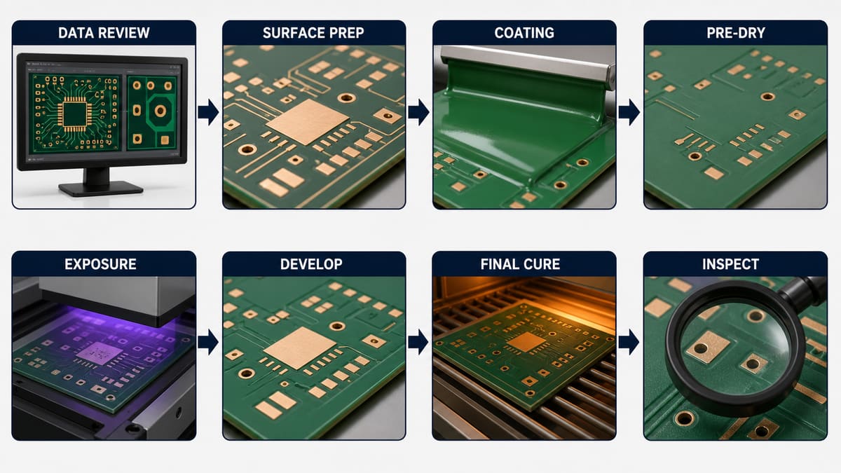
The continuous process below converts mask design data into a cured coating. A defect created early may appear only after development or assembly, so the factory should control causes rather than sort finished boards.
1. Data and manufacturability review. CAM compares the mask layers with copper, drills, vias, board outline and fabrication notes. It checks opening expansion, minimum mask dams, plugged or tented vias, connector areas and exposed copper. Ambiguous positive/negative data can open the wrong area or cover a solderable pad.
2. Surface preparation. Panels are cleaned and micro-prepared to remove oxidation, residues, fingerprints and particles while creating a suitable surface for adhesion. Contamination can cause pinholes, fisheyes or local lifting; aggressive preparation can damage fine copper or change the surface beyond the approved process.
3. Coating application. Liquid mask is applied by the approved screen, curtain, spray or other controlled method. Viscosity, panel topography, coating method and handling influence coverage. Thin areas over trace edges may expose copper; excessive pools can complicate drying and imaging.
4. Pre-dry or tack cure. Controlled heating removes the required solvent and makes the coating stable enough to image without completing the final cure. Under-drying can cause sticking, movement or poor development. Over-drying can reduce developability and leave unwanted mask in openings.
5. Registration and exposure. The panel is aligned to its copper features and selectively exposed using phototool artwork or direct imaging. Exposure cross-links the intended mask areas. Registration error narrows pads or dams; insufficient or excessive exposure changes image fidelity and later development.
6. Development. Unexposed material is removed under a controlled development process, revealing pads, holes and other specified openings. Time, chemistry, spray action and rinse affect the result. Incomplete development leaves residue on solderable surfaces; overdevelopment can attack fine features or reduce mask dimensions.
7. Post-development inspection and touch-up decision. Operators or automated systems check openings, dams, pinholes, particles, scratches and registration before final cure. This is the practical containment point: uncured panels may be reprocessed only under an approved route, while an unrecorded manual touch-up can create a different reliability risk.
8. Final cure. The mask receives the material supplier’s approved thermal and/or UV cure so adhesion, hardness, chemical resistance and electrical properties develop. Cure is a material process, not simply “baking longer.” An incorrect profile can leave the coating soft, brittle, discolored or poorly bonded.
9. Final inspection and downstream release. The factory verifies coverage, pad exposure, registration, surface condition and specified performance evidence. It then releases the panel for legend, surface finish, routing or the next approved operation. Defects near fine-pitch pads receive greater attention because they can directly affect stencil printing and solder bridging.
What Data Must Define the Solder Mask?
| Input | Decision controlled | Risk if missing |
|---|---|---|
| Top/bottom mask layers | Every opening and covered area | Covered pad or unintended exposed copper |
| Fabrication drawing | Material, color, via treatment and notes | Conflicting assumptions |
| Copper and drill data | Registration to pads, vias and holes | Narrow dams or misaligned openings |
| Critical land/connector map | High-risk inspection locations | Functional features treated cosmetically |
| Acceptance specification | Permitted repairs and defect boundaries | Supplier and buyer judge differently |
Use one released dataset and clearly state whether vias are tented, plugged, filled or opened. If a prototype changes those choices, document the deviation in the PCB prototyping process record.
How Do Mask Registration and Dams Affect Assembly?
Registration determines whether the developed opening is centered on the intended land. A shifted opening can reduce available solderable area, expose adjacent copper or remove the dam between pads. At fine pitch, the remaining mask sliver must be manufacturable after imaging and development—not merely visible in CAD at nominal geometry.
Mask-defined pads and copper-defined pads behave differently in assembly and should be intentional. Stencil design, paste release, package requirements and board capability must be considered together. The newly published PCB SMT assembly process guide shows how mask and land decisions influence printing, inspection and solder defects.
What Causes Common Solder Mask Defects?
| Defect | Likely controls to investigate | Buyer evidence |
|---|---|---|
| Pinholes/fisheyes | Surface contamination, particles, coating flow | Magnified coverage inspection |
| Mask on pad | Data polarity, registration, exposure or development | Pad-opening comparison to released data |
| Exposed copper beside trace | Thin coating, edge coverage or misregistration | Optical inspection at critical geometry |
| Peeling/blistering | Cleaning, adhesion, moisture or cure | Adhesion/performance test per requirement |
| Cracks/brittleness | Material, cure, mechanical or thermal stress | Process record and post-stress inspection |
| Residue in opening | Pre-dry and development control | Clean-pad inspection before finish |
How Do Material Type and Color Change the Process?
LPI, dry-film and specialty masks have different coating, imaging and cure routes. Flexible boards, high-temperature use, direct imaging and special colors require material/process compatibility review. A material’s qualification does not automatically qualify every thickness, cure, board construction or end environment.
Color affects optical contrast, inspection behavior and process window; it is not a reliable ranking of electrical quality. Green is common because manufacturing and inspection processes are mature, but another color can be acceptable when the supplier has a controlled material route and the project confirms visual and functional requirements.
What Tests Verify Solder Mask Quality?
Production inspection typically includes visual or automated checks for coverage, registration, openings, pinholes, scratches, repair and contamination. Critical dimensions can be measured against drawing datums. Material/process qualification or product requirements may add adhesion, cure, hardness, solder/chemical resistance, insulation, thermal-stress or environmental tests.
Reference the applicable specification and end-use requirement rather than requesting “IPC compliant” without a document, revision, class or acceptance condition. IPC-SM-840 addresses permanent solder-mask qualification and performance, while bare-board acceptability still depends on the applicable board specification and procurement documentation.
When Should a Mask Defect Be Repaired or Rejected?
The decision depends on location, exposed conductor, minimum spacing, assembly interface, repair material and customer acceptance. A cosmetic mark over laminate is not equivalent to missing mask between fine-pitch conductors. Repairs near connector contacts, impedance features, high-voltage spacing or solder lands require explicit review.
Ask whether repair is allowed, how it is identified, whether the repair receives equivalent cure and inspection, and whether records remain traceable. Uncontrolled touch-up can hide the defect while changing thickness, adhesion or assembly access.
How Do You Choose a Solder Mask Supplier?
- Can CAM reconcile mask, copper, drill and via-treatment data before coating?
- Which material and imaging route will be used, and is it compatible with the board?
- How are cleanliness, coating, pre-dry, exposure, development and cure controlled?
- What inspection targets critical pads, dams and exposed copper?
- Which repairs are allowed and how are they documented?
- What test evidence accompanies special reliability requirements?
Also confirm downstream compatibility with the chosen finish. For example, our immersion tin surface-finish guide explains a separate process that acts on the copper intentionally left exposed.
Frequently Asked Questions
Is solder mask always green?
No. Several colors and material systems exist. Select by qualified process, inspection needs and end-use requirements rather than appearance alone.
Is solder mask electrically insulating?
It is a dielectric coating, but design clearances should not be reduced by assuming the mask can replace required spacing without an approved engineering basis.
What is LPI solder mask?
Liquid photoimageable mask is coated as a liquid, pre-dried, selectively exposed, developed and finally cured.
Why is solder mask found on a pad?
Possible causes include wrong mask data, registration error, exposure/development problems or an intended mask-defined-pad design. Compare with released files first.
What is a solder mask dam?
It is the remaining strip of mask between adjacent openings. It helps separate solderable areas but must be wide enough for the supplier’s process to produce reliably.
Can vias be covered with solder mask?
Vias may be tented, plugged, filled or left open depending on design and process. State the requirement explicitly because these terms are not interchangeable.
How is solder mask inspected?
Use visual/automated inspection, magnification and dimensional checks, plus specified material or performance tests where required.
What files are needed for quotation?
Send the complete PCB data, mask layers, drawing, via treatment, material/color, critical features and acceptance requirements.
Request a Solder Mask DFM Review
Send PCBTRY your Gerber or ODB++, drill data, fabrication drawing, stackup, solder-mask requirements, via treatment and critical pad/dam notes. We can review data consistency, registration risk, material route and inspection evidence before quotation and production.



0 Comments