Blog
Multilayer PCB Manufacturing Process: Registration, Lamination and Testing
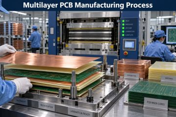
See how multilayer PCBs are fabricated from stack-up and inner layers through lamination, drilling, plating, inspection and electrical testing.



See how multilayer PCBs are fabricated from stack-up and inner layers through lamination, drilling, plating, inspection and electrical testing.
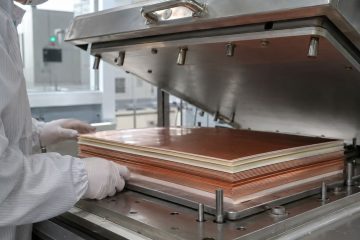
Learn how high-frequency multilayer PCBs are laminated, including material compatibility, surface preparation, registration, press control and post-lamination RF checks.
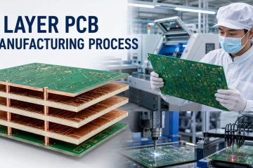
Follow the 4 layer PCB manufacturing process from DFM and inner-layer imaging through lamination, plating, inspection and electrical testing.
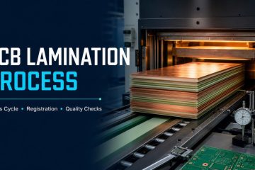
Learn how multilayer PCB lamination controls prepreg, resin flow, vacuum, temperature, pressure, registration, thickness, voids and delamination.
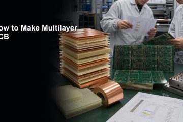
See how multilayer PCBs are designed, imaged, laminated, drilled, plated, finished, and tested, plus the files and DFM checks needed before fabrication.
Learn how multilayer PCB boards are made, from stackup and inner layers to lamination, drilling, plating, testing and buyer DFM checks.
If you have any enquiry about quotation or cooperation, please feel free to email us at [email protected] or use the following enquiry form. Oursales representative will contact you within 24 hours. Thank you for your interest in our products.