




A 4 layer PCB manufacturing process builds two internal copper layers between two external copper layers, creating a bonded structure that can support denser routing, reference planes, power distribution, and more controlled signal return paths than a two-layer board. Manufacturing adds inner-layer imaging and inspection, precise lay-up, lamination, multilayer registration, hole-wall preparation, and plated interconnection to the normal outer-layer process.
PCBTRY can review the proposed stackup, Gerber or ODB++ data, drill files, impedance requirements, material notes, copper weights, finished thickness, surface finish, and inspection plan before production. Send the complete package through the PCBTRY contact page for engineering review and quotation.
What Is a 4 Layer PCB Manufacturing Process?
It is the controlled sequence that converts four separate copper circuit layers into one electrically tested bare board. A common rigid construction starts with a double-sided core for layers 2 and 3, adds prepreg and outer copper foil, laminates the stack, drills and plates interconnections, patterns the outer layers, and completes mask, finish, profiling, and test.
The exact build is not universal. Core thickness, prepreg construction, copper distribution, impedance needs, via structure, finished thickness, resin demand, and the manufacturer’s qualified material set determine the production traveler. The fabrication drawing and approved stackup—not a generic online diagram—must control the order.
When Should You Choose Four Layers Instead of Two?
Choose four layers when the design benefits from dedicated reference or power structures, higher routing density, shorter return paths, better separation of functions, or a more controlled impedance geometry. Four layers do not automatically fix EMC, power integrity, or thermal problems; the layer assignment and routing must use the extra copper intelligently.
A two-layer board may remain appropriate for simple, low-density circuits. Compare electrical risk, layout time, board area, jumper count, assembly difficulty, test access, and expected redesign cost—not only the bare-board quotation.
How Does the 4 Layer PCB Manufacturing Process Work?
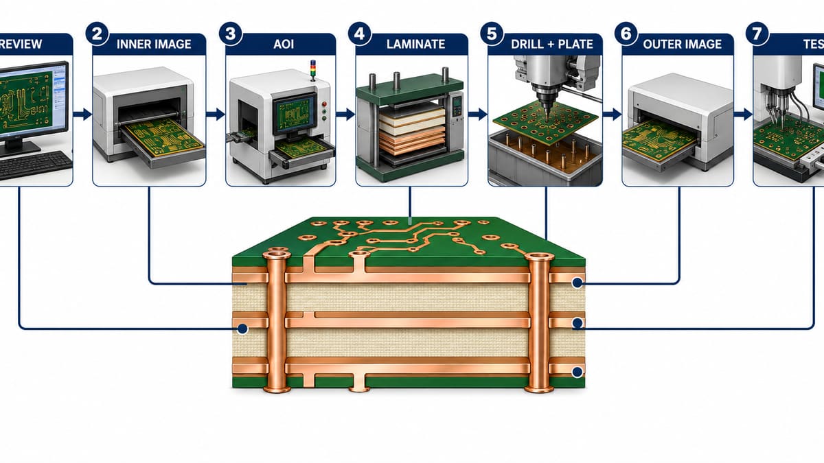
The continuous factory route starts with data review and ends with a released, tested board. Each stage changes what can still be corrected, so defects should be detected before the next irreversible operation.
1. Engineering review and CAM preparation. Engineers reconcile the four copper layers, drill spans, mask, legend, outline, stackup, finished thickness, impedance notes, material, copper weights, finish, dimensions, revision, and test data. CAM outputs drive imaging, drilling, routing, AOI, and electrical test. A mismatched drill revision or ambiguous layer order can create a correctly processed but electrically wrong board, so the buyer should approve resolved questions before release.
2. Material preparation and inner-layer imaging. The selected core is cleaned and coated with photoresist. Direct imaging or phototool exposure transfers layers 2 and 3 to opposite sides. Exposure, registration, surface condition, resist adhesion, and artwork compensation control the image. Weak resist can create opens; residual resist or poor development can leave shorts.
3. Inner-layer etching and AOI. Unwanted copper is removed and the resist is stripped. AOI compares the etched internal circuitry with CAM data for opens, shorts, nicks, protrusions, and spacing anomalies. This is a critical gate because an undetected inner-layer defect becomes inaccessible after lamination and can force rejection of the completed panel.
4. Oxide treatment, lay-up, and registration. The inspected core surfaces are prepared for bonding. Operators or automated systems arrange outer copper foil, prepreg, the inner core, and process materials in the approved order. Layer orientation, tooling targets, cleanliness, prepreg batch, and copper balance matter. Reversing an inner layer or trapping contamination can destroy electrical function or bond integrity.
5. Lamination. Heat and pressure cause prepreg resin to flow, fill the construction, and cure into the bonded four-layer panel. The press cycle must suit the material system and panel design. Excess or insufficient resin flow, trapped gas, uneven copper distribution, contamination, or incorrect pressure/temperature history can contribute to thickness variation, voids, delamination, registration shift, or warpage.
6. Drilling and hole-wall preparation. CNC drilling creates through holes and vias using registered targets. Tool condition, entry/backup material, stack height, spindle behavior, feed, and material movement affect position and hole quality. Hole walls are then prepared to remove drilling residue and expose clean copper at the internal-layer interfaces. Poor preparation can weaken the later copper connection.
7. Electroless copper and electrolytic plating. A thin conductive deposit establishes continuity on the prepared hole wall, then electrolytic copper builds the required conductor. Chemistry, agitation, current distribution, hole geometry, aspect ratio, and process time affect coverage. Voids or insufficient copper at the inner-layer junction can create intermittent or field failures that surface inspection cannot prove absent.
8. Outer-layer imaging, pattern plating, and etching. Layers 1 and 4 are imaged, copper is built where required, an etch resist is applied, and unwanted outer copper is removed. Registration must align the holes, pads, and both outer images. Under-etch can leave shorts; over-etch can narrow traces and annular lands.
9. Solder mask, legend, and surface finish. Solder mask protects copper and defines solderable openings. Legend supports assembly and traceability. The specified finish protects exposed pads and prepares them for assembly. Mask registration, surface preparation, cure, finish coverage, and pad flatness are checked against the approved requirement.
10. Profiling, electrical test, inspection, and packing. Routing, scoring, or another approved method creates the final outline or delivery panel. Electrical test verifies continuity and isolation against the netlist. Dimensional, visual, hole, finish, cleanliness, marking, thickness, warpage, and documentation checks follow the purchase specification before packing.
What Materials Are Used in Four-Layer PCB Manufacturing?
A typical rigid four-layer board uses a copper-clad core, prepreg, and outer copper foil. The material family, glass styles, resin system, copper type and weight, finished thickness, thermal behavior, electrical loss, expansion, flammability requirement, and assembly temperature must suit the application.
Material equivalence should never be assumed from a generic “FR-4” label. If a specific brand, grade, Dk/Df target, Tg class, halogen requirement, thermal characteristic, or approved substitution rule matters, state it in the procurement package and require confirmation.
How Is a 4 Layer PCB Stackup Designed?
A four-layer stackup assigns electrical functions and physical spacing together. The designer and fabricator should agree on layer order, dielectric thicknesses, copper weights, total thickness, material system, impedance geometry, and via structure before artwork release.
| Stackup decision | Manufacturing effect | Buyer check |
| Layer assignment | Controls which copper is imaged internally and externally | Confirm layer order and polarity in CAM review |
| Core and prepreg | Controls bonding, thickness, resin flow, and impedance geometry | Approve an actual manufacturable build |
| Copper distribution | Influences etching, resin demand, and warpage tendency | Review large imbalances and copper thieving assumptions |
| Dielectric spacing | Affects impedance and plane coupling | Provide targets and reference layers, not only trace widths |
| Via spans | Changes drill, plating, and possibly lamination sequence | Identify through, blind, buried, or filled structures explicitly |
What Are the Main Four-Layer Manufacturing Challenges?
The central challenges are preserving inner-layer geometry, aligning all four copper layers, achieving a void-free bonded structure, forming reliable plated interconnections, controlling finished thickness/warpage, and proving hidden features through suitable inspection.
| Risk | Control point | Useful evidence |
| Inner-layer open or short | Imaging, etching and AOI before lay-up | AOI disposition and electrical test |
| Layer misregistration | Tooling, scaling, lay-up and drill targeting | Registration/coupon or microsection evidence when specified |
| Void or delamination | Material storage, cleanliness and lamination cycle | Process traceability and required acceptance inspection |
| Hole-wall connection failure | Drilling, desmear and plating control | Electrical test plus microsection/coupon where required |
| Warpage or thickness error | Symmetry, copper balance, material and press control | Dimensional/thickness/flatness record per specification |
How Does Design Affect Reliability and Yield?
Design controls the process margin available to the factory. Trace/space, annular lands, drill-to-copper clearance, via geometry, copper balance, plane splits, thermal reliefs, solder-mask dams, outline clearance, and impedance structures should fit the selected fabricator’s confirmed capability.
Check return paths when signals change layers, avoid routing critical signals across discontinuous references, and do not use a power-plane arrangement simply because it appears in a generic template. For manufacturability, review dense via fields, narrow neck-downs, heavy/light copper imbalance, routed features near copper, and conflicting finished-hole notes.
What Tests Confirm Four-Layer PCB Quality?
No single test proves every feature. Inner-layer AOI checks circuitry before lamination; electrical testing checks finished-board opens and shorts; dimensional and visual inspection cover outline, holes, mask, finish and marking; microsection or coupon evaluation can examine plated-hole and layer construction when the purchase plan requires it. Impedance testing requires suitable coupons and agreed targets.
Define the acceptance evidence before quotation. Asking for a test report after production may reveal that the required coupon, sampling plan, or traceability was never built into the job.
How Long Does Four-Layer Manufacturing Take?
Lead time depends on file readiness, material availability, stackup confirmation, panelization, impedance work, via complexity, finish, testing, documentation, quantity, factory loading, and whether first-article approval is required. A four-layer board adds inner-layer processing and lamination compared with a basic two-layer route.
Request a confirmed schedule against the reviewed data set. Prototype, small-batch, and production timing should include engineering questions, material procurement, fabrication, testing, documentation, packing, and shipping rather than only machine time.
What Should Be Included in a Four-Layer PCB RFQ?
- Gerber X2 or ODB++ data for all four copper layers, mask, legend, and outline.
- NC drill/route data with plated and non-plated features identified.
- Approved or proposed stackup, finished thickness, copper weights, and material requirements.
- Impedance targets with layer, trace type, reference layer, and coupon/test expectations.
- Surface finish, solder mask, legend, panelization, edge, and via-treatment requirements.
- Dimensions, tolerances, workmanship class/specification, inspection, test, traceability, and report requirements.
- Revision, quantity, schedule, assembly constraints, and any approved substitution rules.
How Do You Choose a Reliable Four-Layer PCB Manufacturer?
Choose a supplier that can turn your electrical intent into an approved, manufacturable stackup; explain its inner-layer AOI, lamination, drilling, hole-wall preparation, plating, electrical test, and traceability controls; and provide evidence matched to the project risk. A generic capability table does not replace a design-specific DFM review.
Ask who owns stackup approval, how engineering questions are documented, what happens when material changes, which features need coupons or microsections, how first articles are controlled, and what the quotation excludes. PCBTRY’s PCB manufacturing service provides a route for file review and comparison quotation when the confirmed build fits the project.
Frequently Asked Questions
What are the four layers in a 4 layer PCB?
They are four conductive copper layers separated by insulating material. Their functions vary; common assignments use external signal layers and internal reference or power layers, but the design must define the actual order.
Does every four-layer PCB use the same stackup?
No. Material availability, thickness, copper, impedance, electrical design and factory process determine the manufacturable construction. Approve the supplier’s actual proposal.
Why is inner-layer AOI performed before lamination?
It checks copper defects while the inner core is still accessible. After lamination, an undetected internal open or short can make the completed panel unusable.
How are vias connected through four layers?
For a standard through via, the laminated panel is drilled, the hole wall is cleaned and activated, and copper is deposited and plated to connect the required layer pads.
Can a 4 layer PCB use blind or buried vias?
It can, but those structures change drill spans and may change the build sequence and cost. Define every span and confirm the supplier’s qualified process before release.
How is layer alignment checked?
Factories use tooling/targets, scaling compensation, imaging alignment, drill registration, inspection data, and—where specified—coupon or microsection evidence. The required proof depends on the purchase specification.
Is electrical testing enough?
No. It verifies continuity and isolation but does not by itself prove laminate identity, bond quality, hole-wall geometry, impedance, dimensions, mask registration, or finish condition.
What files are needed for quotation?
Send all layer data, drill/route files, fabrication drawing, stackup, material and copper requirements, finish, impedance table, tolerances, test/report needs, quantity and revision.
Request a Four-Layer Manufacturing Review
Send the full fabrication package through the PCBTRY contact page. Ask the engineering team to confirm layer order, core/prepreg construction, finished thickness, copper, impedance geometry, via spans, material substitutions, inspection evidence, test scope, quotation assumptions, and production schedule before release.



0 Comments