




The PCB lamination process bonds etched inner-layer cores and prepreg into a multilayer panel under a controlled vacuum, temperature and pressure cycle. Heat makes the prepreg resin flow around copper features; pressure consolidates the stack; curing converts it into a rigid structure. The process is complex because resin flow, material movement, copper distribution and final thickness interact.
PCBTRY reviews the stackup, materials, copper balance, registration targets and special constructions before layup. Send Gerber or ODB++, drill/rout, stackup, material/impedance requirements, finished thickness, quantity and acceptance notes for an engineering review and quotation.
What Is the PCB Lamination Process?
Lamination converts separate cores, copper foils and B-stage prepreg sheets into one bonded panel. It must fill spaces between copper features without trapping voids, starving high-copper regions, shifting layers or exceeding the thickness target. A successful press cycle creates a stable panel for drilling, plating and outer-layer imaging.
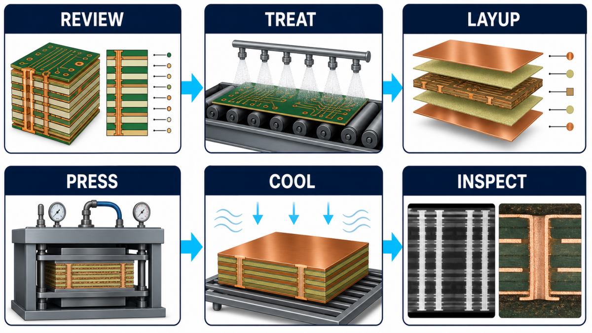
How Does the PCB Lamination Process Work?
1. Stackup and DFM review. Engineering verifies core/prepreg combinations, resin content, copper distribution, thickness and material compatibility. An electrically valid stackup may still be difficult to press if copper density is severely unbalanced or resin demand is underestimated.
2. Inner-layer inspection and treatment. Etched cores are checked for opens, shorts, registration and surface condition, then treated to promote bonding. Contamination or damaged treatment can become interlaminar separation that no later electrical test can reveal.
3. Material conditioning and kitting. Prepreg and cores are controlled for identity, storage condition and moisture exposure. The layup kit follows the released stackup; mixing glass styles, resin systems or orientation changes thickness, flow and electrical behavior.
4. Layup and registration. Operators or automated systems stack cores, prepreg and copper foil using tooling/optical targets. Particles, wrinkles or incorrect orientation create local voids, thickness changes or layer-to-layer offset.
5. Vacuum and press cycle. Vacuum removes trapped air while heat lowers resin viscosity. Pressure consolidates the panel, and the programmed ramp/dwell lets resin fill copper topography before gel and cure. Excess flow can thin dielectric areas; insufficient flow leaves voids or resin-starved zones.
6. Cooling under control. The panel is cooled in a controlled condition before unloading. Uneven thermal history or premature pressure release can increase bow, twist or internal stress.
7. De-pinning, trimming and thickness check. Pressed panels are removed, cleaned and measured. Thickness and flatness data reveal whether the material calculation and cycle behaved as expected.
8. Registration and internal-quality verification. Targets, X-ray, coupons or microsections—selected by construction and specification—confirm layer position, dielectric condition and bond quality before expensive downstream work continues.
How Are Prepreg and Core Materials Selected?
Selection starts with electrical, thermal and reliability requirements, then checks what the fabricator can press consistently. Prepreg glass style and resin content influence dielectric thickness and the amount of resin available to fill copper-free spaces. Core thickness establishes fixed dielectric sections but still moves dimensionally during processing.
Do not substitute prepreg by nominal thickness alone. Resin system, cure compatibility, glass construction, Dk/Df requirement, Tg/thermal performance and availability all matter. The final stackup should state the supplier-approved construction, not an impossible arithmetic total.
How Do Copper Distribution and Resin Flow Interact?
Dense copper areas displace resin; open areas demand more resin. Abrupt density changes can produce local dielectric variation, resin pooling, starvation or thickness gradients. Copper balancing and thieving outside functional areas may improve pressure/flow uniformity, but CAM additions must respect impedance, spacing and customer-controlled zones.
| Condition | Process risk | Engineering response |
|---|---|---|
| Large copper-free window | High local resin demand | Review prepreg resin content and fill distance |
| Solid plane beside sparse signal layer | Unbalanced flow and movement | Balance copper where electrically acceptable |
| Heavy inner copper | More topography to encapsulate | Use a qualified material/press construction |
| Mixed resin systems | Different flow and cure behavior | Require documented compatibility |
What Causes PCB Lamination Defects?
| Defect | Likely contributors | Impact | Evidence |
|---|---|---|---|
| Voids | Trapped air, contamination, poor vacuum or flow | Reduced dielectric/reliability margin | Microsection or agreed nondestructive check |
| Resin starvation | Insufficient resin or excessive squeeze-out | Glass exposure and weak bond | Cross-section and process review |
| Delamination/blister | Moisture, contamination, weak treatment or thermal stress | Layer separation during reflow or service | Thermal stress plus section/analysis |
| Registration error | Material movement, tooling or compensation error | Annular-ring and feature-offset risk | X-ray targets/coupon data |
| Bow and twist | Asymmetric construction or uneven cooling | Assembly handling and soldering problems | Flatness measurement |
| Thickness out of tolerance | Wrong kit, flow or pressure | Connector and impedance mismatch | Panel/board thickness records |
How Does Lamination Affect Registration and Impedance?
Inner layers expand or contract during oxide/treatment and heat exposure. Fabricators apply material- and process-specific scaling so the pressed targets align with later drilling. Poor compensation consumes annular-ring margin even when the drill itself is centered.
Resin flow changes dielectric thickness, which affects impedance. Controlled-impedance designs therefore require a manufacturable construction plus coupon measurement—not only a CAD field-solvers’ nominal value. Review the broader multilayer PCB workflow before freezing the stackup.
How Is Lamination Quality Verified?
Useful evidence includes material/lot traceability, press-cycle records, finished thickness and flatness, X-ray registration, microsection/coupon results, electrical test and any drawing-required thermal stress. The right set depends on board class, via structure, material and risk.
Sequential-lamination HDI adds repeated heat/pressure cycles and tighter registration dependencies. PCBTRY’s HDI manufacturing process explains why microvia build-up cycles need separate review.
How Should Buyers Compare Lamination Capability?
- Can the supplier propose a real material/glass-style stackup rather than a nominal sketch?
- How are prepreg identity, storage and exposure controlled?
- How are copper density and resin demand reviewed before tooling?
- Is the press recipe qualified for the selected material and panel construction?
- How are scaling, registration and thickness measured?
- Which defects trigger hold, review or scrap?
- Can the supplier provide the specified coupon, microsection or traceability report?
Rigid-flex and mixed-material builds require additional interfaces and local pressure/flow controls; see the rigid-flex manufacturing process for that construction.
PCB Lamination FAQ
What does prepreg do in a multilayer PCB?
Prepreg supplies partially cured resin and glass reinforcement. During pressing it flows, fills copper topography and cures to bond adjacent layers.
What causes delamination after reflow?
Moisture, contamination, weak bonding, incompatible materials or excessive thermal stress can contribute. Failure analysis must identify the separation interface.
Can every stackup use the same press cycle?
No. Resin system, prepreg, copper distribution, panel mass and construction affect the qualified recipe.
Why is vacuum used?
Vacuum helps remove trapped air before and during resin flow, reducing void risk. It does not compensate for contaminated materials or insufficient resin.
Does lamination change finished thickness?
Yes. Prepreg flow and copper topography determine the pressed dielectric contribution. The supplier should calculate and verify the final construction.
How is layer registration checked?
Fabricators use tooling/optical targets and may use X-ray or coupons after press. The method depends on construction and required tolerance.
What files are needed for quotation?
Send fabrication data, drill/rout, stackup, finished thickness, material/impedance requirements, copper weights, quantity and required reports.
What adds lamination cycles?
Sequential microvias, buried structures and some mixed-material constructions require repeated build-up. Each cycle adds cost, registration and thermal-history risk.
Request a Lamination DFM Review
Send PCBTRY your fabrication package, stackup, copper weights, material/impedance targets, finished thickness, via structure, quantity and acceptance evidence. Engineering can review resin demand, material compatibility, registration and press-cycle risk before production.



1 Comment
PCB Prototyping Process: DFM, Fabrication and Build Verification - thindry pcb manufacturer · 09/01/2026 at 16:13
[…] without understanding why it existed. Stage-specific reviews also matter; for example, our PCB lamination process guide shows how stackup decisions become factory controls and inspection […]