




Reading a printed circuit board is one of those skills that separates someone who just looks at a green rectangle with random bumps from someone who actually understands what is happening inside a device. Whether you are a junior engineer debugging a prototype, a procurement specialist evaluating a supplier’s build quality, or a hobbyist trying to reverse-engineer a circuit, knowing how to read a PCB gives you a real advantage. This guide walks you through everything — from identifying bare components on a physical board to interpreting schematics, silkscreen markings, copper traces, and layer stacks. Every section is based on real manufacturing experience from a PCB fabrication facility that handles everything from simple two-layer boards to 80-layer server backplanes.
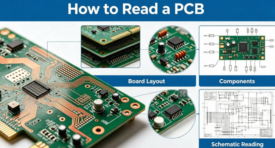
What Exactly Is a PCB and Why Does Reading One Matter
A printed circuit board is the physical platform that mechanically supports and electrically connects electronic components through conductive pathways etched from copper sheets laminated onto a non-conductive substrate. At its simplest, a PCB is a flat board made of fiberglass (most commonly FR-4) with copper traces running across its surface like roads on a map. Components sit on top of or through the board, and the copper traces carry electrical signals between them.
Understanding how to read a PCB matters because it directly impacts design validation, quality inspection, failure analysis, and procurement decisions. When you send a Gerber file to a manufacturer, they fabricate exactly what you specified — but if you cannot read the resulting board yourself, you have no way to verify the output. Engineers who can read PCBs catch design errors before assembly. Quality inspectors who understand board layouts identify defects faster. Buyers who recognize what they are looking at can evaluate supplier quality without depending entirely on third-party reports.
How a PCB Is Structured From Copper to Silkscreen
Before you can read a board, you need to understand what layers make it up. A typical PCB consists of several distinct layers, each serving a specific purpose.
Copper layers carry the electrical signals. A simple single-layer board has copper on one side only. A two-layer board has copper on both the top and bottom. High-density designs like server backplanes or AI accelerator cards can stack 20, 40, or even 80 copper layers, with signals routed on internal planes that you cannot see from the surface.
Substrate is the insulating material between copper layers. Standard FR-4 (a glass-reinforced epoxy laminate) works for most applications. High-frequency boards use specialized materials like Rogers or Taconic. Metal-core PCBs use aluminum or copper substrates for thermal management in LED lighting or power electronics.
Solder mask is the colored coating (usually green, but also black, red, blue, or white) that covers the copper traces. Its job is to prevent accidental short circuits during soldering and to protect copper from oxidation. The solder mask is what gives most PCBs their characteristic green appearance.
Silkscreen is the layer of text, symbols, and markings printed on top of the solder mask. This is the layer you will spend the most time reading. It contains component reference designators (R1, C3, U5), polarity markers, pin-1 indicators, logos, revision numbers, and test point labels. Good silkscreen makes a board easy to assemble and debug. Poor silkscreen makes a board a puzzle.
Solder pads and vias are the exposed copper areas where components attach or where signals transition between layers. Pads come in different shapes — round, rectangular, oval — matching the footprint of the component they hold. Vias are small plated-through holes that connect copper on one layer to copper on another.
The Silkscreen Layer: Your Primary Map for Reading a PCB
When someone says “read a PCB,” they usually mean interpreting the silkscreen. Here is what each marking tells you.
Reference Designators
Every component on a board gets a reference designator — a short alphanumeric code that links the physical part to its position on the schematic. The standard naming convention follows industry practice:
| Prefix | Component Type | Example |
|---|---|---|
| R | Resistor | R12, R204 |
| C | Capacitor | C3, C89 |
| L | Inductor | L1, L5 |
| D | Diode | D2, D10 |
| Q | Transistor | Q4, Q12 |
| U | Integrated Circuit | U1, U23 |
| J | Connector / Jack | J1, J4 |
| SW | Switch | SW1 |
| F | Fuse | F1 |
| Y / X | Crystal / Oscillator | Y1 |
| TP | Test Point | TP1, TP7 |
| FB | Ferrite Bead | FB2 |
When you look at a board and see “U1” surrounded by a square outline with numbers at each corner, you are looking at the primary integrated circuit — usually the microprocessor, FPGA, or main controller. The numbers at the corners are pin-1 indicators. On surface-mount packages, pin 1 is typically marked with a dot, a beveled edge, or a small triangle on the IC package itself, and the silkscreen on the board often shows a corresponding dot or arrow.
Polarity and Pin-1 Markings
Getting polarity wrong during assembly can destroy components instantly. The silkscreen helps prevent this. Capacitors and diodes show a clear polarity indicator — a plus sign (+) for polarized capacitors, a stripe or band for cathode on diodes, and a filled dot or triangle near pin 1 for ICs. LEDs have a clear cathode marking. Electrolytic capacitors usually show a curved line on the negative side. Always check these marks against the schematic before assuming anything.
Board Identifiers and Revision Codes
Nearly every production PCB carries a board name or model number, a revision code (like Rev 1.2 or V2.0), a date code, and often a manufacturer’s logo or UL certification mark. These are important for traceability. If you receive a batch of boards and need to verify revision consistency, the silkscreen is your first checkpoint. A board marked “Rev 1.0” when you ordered “Rev 2.3” means something went wrong in the production routing.
Understanding PCB Copper Traces and Routing
The copper traces visible through or beneath the solder mask are the “wires” of a PCB. Reading them requires a bit of practice, but the basics are straightforward.
Trace width tells you about the current-carrying requirement. Power traces are wide — sometimes several millimeters — because they carry more current. Signal traces are thin, often 0.15mm to 0.2mm for standard digital designs. When you see a noticeably wider copper path on a board, you can usually assume it is part of the power distribution network.
Trace routing follows deliberate patterns. Signals typically run at 45-degree angles rather than 90-degree corners because sharp angles can cause impedance discontinuities at high frequencies. If you see traces that snake back and forth in a controlled zigzag pattern, that is length matching — the designer is ensuring that parallel signals arrive at their destination at the same time, which is critical in high-speed memory interfaces and differential pairs.
Copper pours and ground planes appear as large solid areas of copper rather than individual traces. On a two-layer board, you will often see one layer dedicated mostly to signal routing while the other layer is a near-continuous copper plane serving as ground or power. On multi-layer boards, internal layers are frequently dedicated entirely to ground or power planes, providing low-impedance return paths and electromagnetic shielding.
Thermal relief pads appear as pads connected to a copper plane through short traces rather than a solid connection. This design prevents the large copper plane from wicking heat away too quickly during soldering, making hand soldering or rework possible. Without thermal relief, soldering a through-hole component to a ground plane becomes extremely difficult because the plane acts as a heatsink.
How to Read a PCB Schematic vs. the Physical Board
The schematic is the logical representation of the circuit. The physical PCB is the spatial realization of that logic. Reading one without the other gives you an incomplete picture. Here is how they connect.
A schematic shows every component, every connection, and every electrical relationship in a clean, organized diagram grouped by function. Power supply circuitry is usually shown at the top or left. Signal processing flows left to right. Connectors appear at the edges. The schematic tells you what is connected to what.
The physical PCB tells you where everything is placed and how the connections are routed through physical copper. Two points connected on the schematic might be connected through a via to an internal layer on the PCB — you will not see that connection on the surface.
To read them together, start with the schematic to understand the circuit’s functional blocks. Then locate those blocks on the physical board by matching reference designators. Use a multimeter in continuity mode to verify connections you cannot visually trace. For complex multi-layer boards, the Gerber files or the original CAD layout software is the only reliable way to see internal routing.
Identifying Common PCB Components by Sight
Recognizing components on a physical board without reading the part number is a valuable skill. Here is a practical reference.
| Component | Physical Appearance | Typical Marking |
|---|---|---|
| Resistor (SMD) | Small black rectangular chip | 3-4 digit code or “R” marking |
| Capacitor (Ceramic SMD) | Tan, brown, or gray chip | Usually unmarked on small sizes |
| Electrolytic Capacitor | Cylindrical can, usually vertical | Value, voltage, polarity stripe |
| Tantalum Capacitor | Small colored rectangular body | Value and polarity line |
| Diode | Small cylinder or SMD chip | Cathode stripe or band |
| LED | Transparent or colored lens | Flat edge marks cathode |
| Transistor (SOT-23) | 3-pin small outline package | Part number laser-etched |
| IC (QFP) | Square with pins on all four sides | Pin-1 dot, part number on top |
| IC (BGA) | Flat square, no visible pins (ball grid underneath) | Part number, orientation mark |
| Inductor | Toroid or block shape, sometimes shielded | Value or part number |
| Crystal Oscillator | Metal can or ceramic package | Frequency stamped on top |
| Connector (USB, HDMI, etc.) | Metal shielded housing | Usually unlabeled on board |
| Ferrite Bead | Looks similar to resistor | Marked “FB” or with code |
A common mistake for beginners is confusing small ceramic capacitors with resistors — they look very similar in 0402 or 0603 packages. The reference designator is the most reliable way to tell them apart. When the silkscreen is too small to read, use the schematic as your reference.
Reading Multi-Layer PCBs and Understanding Layer Stacks
Modern electronics rarely use single or double-layer boards. A smartphone motherboard might have 10 to 12 layers. A server GPU card can use 16 or more. An AI training server motherboard may go up to 20 to 80 layers depending on signal density and power distribution requirements.
You cannot read internal layers by looking at a physical board. To understand the layer stack, you need access to the fabrication drawings — specifically the stackup diagram that the PCB designer provides to the manufacturer. This diagram specifies each layer’s copper weight, dielectric thickness, and material type.
Standard notation works like this: a 6-layer board might be described as L1 (top signal), L2 (ground plane), L3 (power plane), L4 (power plane), L5 (ground plane), L6 (bottom signal). The designer selects this arrangement to provide good signal integrity — every high-speed signal on the top layer has an adjacent ground plane on L2 for a clean return path.
When reviewing a multi-layer PCB, the most practical approach is to examine the external layers visually, then use the design files or netlist to understand internal connectivity. This is why experienced engineers always request Gerber files and drill files alongside physical samples during prototype evaluation.
PCB Testing and Inspection Methods for Reading Board Quality
Knowing how to read a PCB is not just about understanding the layout — it is also about evaluating whether the board meets quality standards. Here are the primary inspection methods used in production environments.
Visual inspection is the first line of defense. Trained operators (or increasingly, automated optical inspection machines) examine every board for solder bridges, missing components, tombstoned parts, insufficient solder, silkscreen alignment, and solder mask defects. The IPC-A-610 standard defines the acceptance criteria for each defect class.
Automated Optical Inspection (AOI) uses cameras and image comparison algorithms to check component placement accuracy, solder joint quality, and polarity verification at production speed. Modern AOI systems compare each board against a golden reference or against the centroid data from the design files.
X-ray inspection is essential for ball grid array (BGA) and other packages where solder joints are hidden beneath the component body. X-ray imaging reveals voids, bridging, and insufficient solder in these hidden connections — defects that no optical system can detect.
In-Circuit Test (ICT) uses a bed-of-nails fixture to make contact with specific test points on the board and measure individual component values, verify connections, and detect manufacturing defects. This method is thorough but requires custom fixture design for each board.
Functional testing powers up the board and runs it through its intended operations. This catches design-level issues that manufacturing inspection cannot — a perfectly soldered board can still fail if the firmware is wrong or a component was specified incorrectly.
Industry-Specific PCB Reading Requirements
Different industries impose different standards on PCB design and inspection, which affects how you read and evaluate boards.
Consumer electronics boards — smartphones, wearables, smart home devices — prioritize density and miniaturization. You will see extensive use of HDI (high-density interconnect) technology with microvias, fine-pitch BGAs, and flexible printed circuits (FPC). Reading these boards requires understanding of via-in-pad technology and sequential lamination processes.
Automotive electronics must meet IATF 16949 standards and survive operating temperatures from -40°C to 150°C. Boards in this space use thicker copper, larger component spacing for thermal cycling resilience, and conformal coating for moisture protection. The PCB silkscreen will often include automotive-grade markings and the board will use materials rated for higher glass transition temperatures.
Medical devices require ISO 13485 compliance. Traceability is paramount — every board must be trackable to its manufacturing lot, material batch, and assembly date. Reading a medical PCB means checking not just the layout but also the UL marking, date codes, and any special handling instructions printed on the board.
Industrial and power electronics boards feature thick copper (3oz to 6oz or more) for high-current paths, metal-core substrates for thermal management, and robust through-hole components alongside surface-mount technology. These boards are visually distinct — the copper traces are visibly thicker and heavier than what you see on consumer electronics.
Common Mistakes When Reading PCBs and How to Avoid Them
Even experienced engineers make errors when reading unfamiliar boards. Here are the most frequent pitfalls.
Confusing mirror images. When you flip a two-layer board over, everything is mirrored. Components on the bottom layer appear reversed when viewed from the top. Always confirm which side you are looking at before reading reference designators.
Assuming visible traces are the complete picture. On any board with more than two layers, the majority of connections are invisible. Do not assume a connection does not exist just because you cannot trace it on the surface.
Ignoring the solder mask openings. The solder mask is not just cosmetic — its openings define exactly where solder will adhere. If you see copper that appears exposed but has no solder pad, it might be a test point, an antenna structure, or an intentional keep-out area. Do not assume every exposed copper area is a connection point.
Misidentifying similar packages. Many SMD components look nearly identical from above. A 0402 resistor and a 0402 capacitor are the same physical size. Always cross-reference the designator with the schematic rather than guessing from appearance.
Overlooking thermal features. Copper fills, thermal vias under QFN packages, and large copper areas around power components are all thermal management strategies. They look like general copper pours but serve a critical cooling function. Removing or modifying them during rework can cause thermal failures.
Tools and Resources for Reading PCBs More Effectively
Several tools make PCB reading easier and more accurate.
Magnification is essential for any board with fine-pitch components. A stereo microscope or a good USB digital microscope with at least 20x magnification lets you read tiny silkscreen text, inspect solder joints, and identify component markings that are invisible to the naked eye.
Multimeter in continuity mode lets you verify connections that you cannot visually trace. Touch one probe to a pad and the other to a suspected destination — a beep confirms a connection. This is especially useful for debugging or reverse-engineering a board without the schematic.
Board viewer software like the open-source Gerber viewer tools (GerberView, ViewMate, or online viewers like Tracespace) lets you load Gerber files and examine each layer independently. You can toggle layers on and off, zoom into specific areas, and cross-reference the physical board with its design files.
Schematic capture software (KiCad, Altium, OrCAD, Eagle) allows you to load the schematic file and cross-probe between the schematic and layout. Click a component on the schematic and its physical location highlights on the board layout, and vice versa.
IPC standards documents — particularly IPC-A-610 (Acceptability of Electronic Assemblies), IPC-2221 (Generic Standard on Printed Board Design), and IPC-TM-650 (Test Methods Manual) — provide the authoritative reference for quality criteria and design guidelines.
How PCB Manufacturing Quality Affects Readability
The quality of the manufacturing process directly impacts how easy a board is to read and work with. Poor-quality fabrication creates real problems.
Thin or misaligned silkscreen makes reference designators unreadable. We have seen production batches where the silkscreen registration was off by 0.3mm — enough to shift text off the pad area and make the board frustrating to assemble. High-quality manufacturers use direct legend printing (inkjet) rather than traditional screen printing to achieve tighter registration.
Solder mask registration errors can partially cover pads, making soldering difficult and inspection unreliable. The IPC Class 2 standard allows up to 0.05mm solder mask-to-pad offset, while IPC Class 3 (used in automotive and medical) tightens this considerably.
Copper etching quality affects trace readability. Under-etched traces can create unintended connections. Over-etched traces can create open circuits or increase resistance beyond specification. Cross-section analysis is the definitive way to verify etch quality, but experienced operators can spot obvious etch problems during visual inspection.
Practical Example: Reading a Typical Power Supply PCB
Let us walk through reading a real board type. A switch-mode power supply PCB is one of the most common boards an engineer will encounter, and it illustrates many reading principles well.
Starting at the input connector (J1), you would typically find a fuse (F1) immediately followed by an EMI filter section — common-mode chokes (L1, L2) and X/Y capacitors (C1 through C4). The silkscreen groups these components together, and the schematic shows them as a filtered input stage.
Moving across the board, you find the primary-side switching MOSFET (Q1) mounted near a transformer (T1). The MOSFET is usually the component with the largest heatsink nearby. The transformer is unmistakable — it is the largest magnetic component on the board, with visible wire windings or a bobbin structure.
The secondary side contains output rectifier diodes (D1, D2), output capacitors (C10 through C15 — usually multiple electrolytic caps in parallel for low ESR), and an output inductor (L3). The feedback circuit, often built around a small optocoupler (U2) and a reference IC (U3), connects the secondary output voltage back to the primary-side controller (U1) to regulate the output.
Reading this board tells you the power flow: input → filter → switching stage → transformer → rectification → output filtering → load. This functional-block approach works for virtually any PCB.
How to Choose the Right PCB Manufacturer When You Need Boards You Can Reliately Read
Board readability starts with manufacturing quality, which starts with manufacturer selection. Here are the factors that matter.
Silkscreen quality should be part of your evaluation criteria. Ask for sample photos of completed boards. Check whether the text is sharp, centered on the pads, and legible at the intended font size. Manufacturers using direct legend printing (DLP) or inkjet legend processes produce noticeably sharper silkscreen than traditional screen-printed legends.
Layer count and stackup precision affect internal trace alignment. A manufacturer that regularly builds 20-layer boards with controlled impedance will handle your 4-layer board with consistent quality. Ask about their layer-count capabilities and whether they provide X-ray cross-section reports for impedance-critical orders.
Certifications indicate process maturity. ISO 9001 covers general quality management. IATF 16949 demonstrates automotive-grade process control. ISO 13485 confirms medical device manufacturing capability. UL listing ensures the base materials meet safety standards. These certifications are not just paperwork — they represent documented, audited processes that consistently produce boards you can read and work with.
Design for Manufacturability (DFM) review is a service that separates good manufacturers from commodity suppliers. A thorough DFM review checks silkscreen legibility, solder mask clearances, drill-to-copper spacing, and trace width compliance before fabrication begins. This pre-production step catches readability and manufacturability issues when they are cheap to fix.
How to Read a PCB During Quality Inspection and Incoming Receiving
When boards arrive from a manufacturer, your incoming inspection process should include several readability-related checkpoints.
Verify the board revision matches your order. Check the silkscreen revision code against your purchase order. Count the component footprints against your BOM to confirm all intended placements are present and correctly sized. Inspect solder mask alignment on critical fine-pitch components. For assembled boards (PCBA), verify component polarity markings against the schematic. Sample-check solder joint quality on BGA packages using X-ray if you have the capability, or request X-ray reports from the manufacturer.
Document any discrepancies immediately. A board with illegible silkscreen, misaligned solder mask, or incorrect revision markings should be flagged before it enters your assembly line or product integration stage.
Global PCB Sourcing: What International Buyers Need to Know About Reading Boards
If you are sourcing PCBs from overseas manufacturers — and most of the world’s PCB production capacity is concentrated in China — understanding how to read and evaluate boards remotely becomes even more important.
Request comprehensive fabrication drawings with your order. These include the layer stackup diagram, drill chart, copper weight specifications, surface finish type (HASL, ENIG, immersion silver, OSP), and silkscreen requirements. Without these documents, you have no baseline for evaluating the delivered product.
Ask for pre-production verification photos — copper patterns, drill accuracy, silkscreen registration — before the manufacturer proceeds to full production. Most reputable Chinese manufacturers will provide these as part of their standard communication process.
For assembled boards, request component placement photos from multiple angles, X-ray images of BGA packages, and AOI inspection reports. A manufacturer willing to provide transparent documentation is a manufacturer confident in their process.
Frequently Asked Questions
How do I read the value of an SMD resistor on a PCB?
Small surface-mount resistors use a numeric code printed on top. A three-digit code like “472” means 47 × 10² = 4,700 ohms (4.7kΩ). A four-digit code like “4702” means 470 × 10² = 47kΩ. For very low values, an “R” replaces the decimal point — “4R7” means 4.7 ohms. Precision resistors below 10 ohms may use a different system. If the code is too small to read, use the schematic or a multimeter in resistance mode.
What is the difference between reading a PCB layout and reading a schematic?
A schematic shows the logical electrical connections between components — which pin connects to which, organized by function. A PCB layout shows the physical placement of components and the actual copper routing between them on the board. The schematic tells you what the circuit does. The layout tells you where everything physically sits. You need both to fully understand a board.
Why are some PCB traces wider than others?
Wider traces carry more current. Power supply rails, ground connections, and motor driver outputs use wide traces to minimize resistance and prevent overheating. Thin traces carry low-current signals where space is at a premium. The trace width is calculated based on the current it must carry, the allowed temperature rise, and the copper thickness — a process governed by IPC-2221 standards.
How can I identify which layer a trace is on when looking at a physical board?
You can only see the outermost copper layers (top and bottom) directly. Internal layers are hidden. For the outer layers, use a multimeter in continuity mode to probe connections, or load the Gerber files in a board viewer to examine each layer independently. If you do not have design files, reverse-engineering a multi-layer board requires X-ray inspection for internal layers.
What does “ENIG” mean on a PCB specification, and why does it affect readability?
ENIG stands for Electroless Nickel Immersion Gold — a surface finish where a thin gold layer is deposited over nickel on exposed copper pads. ENIG produces a flat, uniform surface that is excellent for fine-pitch components and wire bonding. It also provides good contrast against the solder mask, making pads easy to identify during inspection.
Can I read a PCB without the original schematic?
Yes, but with limitations. You can identify components by their reference designators, package types, and markings. You can trace visible connections with a multimeter. For simple two-layer boards, you can reconstruct most of the circuit. For multi-layer boards, internal connections are invisible without X-ray or design files. Reverse engineering is possible but time-consuming.
How do I identify a BGA component’s orientation on a PCB?
BGA (Ball Grid Array) packages have an orientation mark — usually a dot, triangle, or beveled corner on the package body. The silkscreen on the PCB mirrors this mark with a corresponding indicator near pin 1. Additionally, many BGAs have a small notch or chamfered edge that indicates pin-1 location. Always cross-reference with the schematic or datasheet.
What makes a PCB silkscreen hard to read, and how do manufacturers prevent it?
Common causes include excessive component density, small font sizes (below 0.8mm), poor registration alignment, and low-contrast color choices. Quality manufacturers use minimum 0.8mm font heights, ensure silkscreen does not overlap solder pads, choose high-contrast color combinations (white on green or black), and use inkjet or laser direct imaging for precise legend placement.
How do I verify that a received PCB matches my design files?
Compare the physical board against your Gerber files layer by layer. Check trace routing, pad locations, drill positions, and silkscreen content. Use a microscope for fine details. Verify the board dimensions and outline match. For assembled boards, cross-check every component reference designator and value against the BOM. Request the manufacturer’s AOI and electrical test reports as additional verification.
What is a test point, and how do I identify them on a PCB?
Test points are small exposed copper pads (sometimes labeled “TP1,” “TP2,” etc.) placed intentionally on a board for probing during production testing or field debugging. They connect to specific net nodes so technicians can measure voltages, signals, or continuity without soldering wires. They are usually round pads, unmasked, and clearly labeled on the silkscreen.
Why do some boards have copper on the edge of the board?
Copper near the board edge can serve several purposes: it may be part of the ground plane extending for shielding, an antenna structure, or a thermal management feature. However, copper too close to the board edge (within 0.5mm) can cause problems during routing or V-scoring — the cutting process can nick the copper and create short circuits. Proper design keeps copper at least 0.3-0.5mm from any board edge.
How does the choice of solder mask color affect PCB readability?
Green solder mask provides the best contrast for both visual inspection and automated optical inspection. White solder mask is common in LED boards for light reflection but makes white silkscreen text very hard to read — manufacturers switch to black silkscreen in those cases. Black solder mask looks sleek but makes trace inspection difficult. Red and blue masks are used for branding but do not significantly affect readability.
What role do fiducial markers play when reading or assembling a PCB?
Fiducials are small, precisely placed copper circles (usually 1mm diameter) on the board surface, surrounded by a solder mask opening. They serve as reference points for pick-and-place machines and AOI systems. The machine’s camera locates these fiducials to calculate the board’s exact position and orientation before placing components. Without fiducials, automated assembly accuracy drops significantly.
How do I interpret impedance test results on a high-speed PCB?
Impedance test coupons — small test structures fabricated alongside your actual board — are measured using a time-domain reflectometer (TDR). Results are compared against the target impedance specified in your design (commonly 50Ω single-ended or 100Ω differential). Deviation beyond ±10% typically indicates a fabrication issue with dielectric thickness, trace width, or copper etching. Request impedance test reports from your manufacturer for any high-speed design.
What should I check first when a newly assembled PCB does not power on?
Start with visual inspection: look for missing components, solder bridges, reversed polarity, and cold solder joints. Then check power input with a multimeter. Verify that voltage regulators output the correct voltages. Inspect solder joints on the main IC and any BGA packages — these are the most common assembly failure points. If the board uses a microcontroller, verify that the crystal oscillator is running and that the reset pin is not stuck in the reset state.
Understanding how to read a PCB is a foundational skill that pays dividends across design, manufacturing, quality, and procurement. The more fluently you can interpret what you see on a board, the faster you can identify problems, validate quality, and communicate effectively with your manufacturing partners.
If you are sourcing reliable PCB or PCBA manufacturing — whether for prototyping, mass production, OEM, ODM, or custom engineering solutions — reach out to our engineering team for technical support and a quote at [email protected].



1 Comment
How to Cross-Check a PCB Schematic Against the Physical Board - thindry pcb manufacturer · 08/26/2026 at 08:28
[…] How to Read a PCB for physical layout and component-reading fundamentals. […]