




You’ve probably read a dozen articles that start with “PCB potting is the process of encapsulating electronic assemblies in a protective compound.” That sentence is accurate. It’s also completely useless for deciding whether you should actually do it.
Let’s skip the definition and go straight to the questions that actually matter — the ones that show up on engineering forums at 2 AM when someone’s staring at a board that just failed its third humidity test, or when a hobbyist is trying to waterproof an Arduino project for a garden sensor and doesn’t want to spend $500 on materials.
What Potting Actually Does
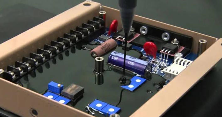
Take a finished PCB assembly. Put it in a housing or mold. Pour a liquid compound over it until every component, every trace, every solder joint is completely submerged. Wait for it to cure into a solid. That’s potting.
The result is a board that’s literally encased in a block of material. There are no air gaps, no exposed copper, no accessible components. Water, dust, vibration, chemicals, salt spray — none of it can reach the electronics because there’s nothing to reach. The air that used to surround every component has been replaced with a solid barrier.
That’s a fundamentally different approach from conformal coating, which paints a thin film over the surface of the board. Coating follows the contours of the assembly. Potting buries it. The distinction matters more than most people realize, and choosing between them is one of the first real decisions you’ll face.
Potting vs. Conformal Coating: How to Actually Decide
I see this question come up constantly, and the answers people give are usually too vague to be useful. So here’s a framework that might actually help.
Choose conformal coating when:
- Your product lives indoors in a reasonably controlled environment
- You need to be able to access components for rework or repair
- Weight is a concern — coating adds almost nothing, potting adds grams to kilograms
- Cost per unit matters and the protection requirements are moderate
- Testing and inspection after application are important — you can still probe through coating in many cases
Choose potting when:
- The board will face full water submersion or sustained high-humidity exposure
- Mechanical shock and vibration are significant factors — automotive under-hood, marine, industrial machinery
- You need chemical resistance beyond what coating can provide
- Electrical insulation at high voltages is required — potting fills all the gaps between traces and components
- Thermal management through conduction to the housing is part of the cooling strategy
- The product is permanently installed and will never need field repair
The hard truth: if there’s any chance you’ll need to open the enclosure and rework the board after assembly, think very carefully about potting. It’s essentially a one-way door. Once you pour, getting back in is messy, expensive, and sometimes impossible without destroying the board. I’ve watched teams throw away perfectly functional assemblies — just because the BOM was wrong and the compound was already cured.
For a quick visual summary of how the two methods compare across key parameters:
| Factor | Potting | Conformal Coating |
|---|---|---|
| Water protection level | Submersion capable | Splash and humidity only |
| Mechanical protection | Excellent — full encapsulation | Minimal |
| Weight impact | Significant | Negligible |
| Accessibility after application | None without removal | Limited but possible |
| Thermal conductivity | High (conduction to housing) | None |
| Cost per board | $2 – $30+ depending on compound and volume | $0.50 – $5 |
| Rework difficulty | Very difficult | Moderate |
The Three Main Compound Types — And When Each One Actually Matters
Here’s where most guides give you a table of properties and call it a day. The problem is that properties don’t tell you much unless you know what environment you’re designing for. So instead of just listing specs, let me walk through the real tradeoffs.
Epoxy — The Default Choice (Until It Isn’t)
Epoxy is what most people reach for first. It’s rigid, chemically resistant, adheres well to most substrates, and can be formulated with thermally conductive fillers to reach 1.0 to 2.5 W/(m·K) — that’s 40 to 100 times better than air at 0.025 W/(m·K).
Here’s what people don’t tell you about epoxy:
The exotherm problem is real. When epoxy cures, it generates heat. For thin layers or small volumes, this doesn’t matter much. But if you’re potting a board in a deep enclosure — say, more than 20mm of compound in one pour — the center temperature can spike to 80–120°C during cure. That’s hot enough to damage plastic connectors, crack ceramic capacitors, or push electrolytic capacitors past their rated temperature. I’ve personally seen 0805 ceramic caps crack from exothermic stress in a thick epoxy pour. The board looked fine during visual inspection but failed electrical test afterward.
CTE mismatch causes long-term problems. Standard epoxy has a coefficient of thermal expansion around 55–80 ppm/°C. Your FR-4 board is roughly 14–17 ppm/°C in the X-Y plane. That’s a 4x to 5x difference. Over hundreds of thermal cycles — which is nothing for an automotive or industrial product — that mismatch creates stress at every interface. Solder joints crack. The compound delaminates from the board. Traces lift. Low-CTE epoxy formulations exist (down to 20–30 ppm/°C), but they cost more and are harder to process.
Best for: industrial controls, power supplies, fixed-installation equipment, anything that lives in a box and doesn’t move much.
Polyurethane — The Compromise That Usually Works
Polyurethane stays somewhat flexible after cure. It doesn’t have the rigid armor-like quality of epoxy, but it handles thermal expansion mismatch far better because it can absorb the stress instead of cracking under it.
It also cures at room temperature and is more tolerant of moisture during the cure process. Epoxy can absorb atmospheric humidity and develop bubbles during cure — polyurethane is more forgiving in this regard, which matters if you’re not working in a controlled environment.
The tradeoff: lower chemical resistance than epoxy, and weaker adhesion to certain substrates. If your application involves fuel, solvents, or aggressive chemicals, epoxy or silicone might be better choices.
Best for: automotive electronics, outdoor installations, applications with wide temperature swings, situations where some flexibility is valuable.
Silicone — Premium Performance, Premium Price
Silicone is the material you choose when the environment is genuinely hostile. It remains flexible from roughly -55°C to +200°C (sometimes higher with specialty formulations), doesn’t yellow under UV exposure, and is inherently flame-retardant without the halogenated additives that some epoxy and PU compounds require.
It also has the lowest CTE of the three — typically 200–300 ppm/°C, which sounds high, but because it’s so soft and flexible, that expansion doesn’t create the same mechanical stress that a rigid epoxy at 60 ppm/°C would. It’s counterintuitive, but flexibility solves the thermal expansion problem even with a higher numerical CTE value.
The downside: it’s expensive. Often 3 to 5 times the cost of epoxy per kilogram. It also has lower mechanical strength and lower thermal conductivity in standard formulations (around 0.2–0.3 W/(m·K)). Thermally conductive silicone compounds exist, but they push the cost even higher.
Best for: aerospace, LED lighting, marine electronics, any application where the board will see extreme temperature cycling or prolonged UV exposure.
Quick Material Comparison
| Property | Epoxy | Polyurethane | Silicone |
|---|---|---|---|
| Rigidity after cure | Hard / rigid | Semi-flexible | Soft / flexible |
| Thermal conductivity | 0.2 – 2.5 W/(m·K) | 0.2 – 0.5 W/(m·K) | 0.2 – 0.4 W/(m·K) |
| Typical operating range | -40°C to +150°C | -40°C to +120°C | -55°C to +200°C |
| UV resistance | Poor (yellows) | Moderate | Excellent |
| Chemical resistance | Excellent | Moderate | Good |
| Mechanical shock absorption | Poor (rigid) | Good | Excellent |
| Exothermic heat during cure | High (watch out!) | Low to moderate | Very low |
Design Considerations: What Potting Changes About Your Board
Potting isn’t something you bolt on at the end of a project. It changes your thermal design, your test strategy, your mechanical layout, and your manufacturing process. If you don’t plan for it early, you’ll regret it.
Thermal Management
This is the one that bites people the hardest. Convection cooling — fans, open enclosures, airflow — stops working the moment you fill the air space with solid compound. All heat now flows by conduction through the potting material to the housing, and from there to the ambient environment.
The math is straightforward but unforgiving. The thermal resistance of a potting layer is:
Rth = t / (k · A)
where t is the thickness of the compound layer, k is its thermal conductivity, and A is the cross-sectional area of the heat path. If k is low (standard silicone at 0.2 W/(m·K)) and t is large (thick layer between the component and the housing wall), thermal resistance goes up fast. Your junction temperatures rise accordingly.
The practical takeaway: if you’re potting anything with significant power dissipation, you need to specify a thermally conductive compound and minimize the distance between hot components and the housing wall. Some teams design the board layout specifically around this — placing power components on the side closest to the heatsink wall and orienting the board so the potting path is as short as possible.
Test Points and Debug Access
Every test point, every header, every debug connector needs to be planned before potting. Once the compound is cured, you cannot probe a pad with a multimeter. You cannot attach an oscilloscope clip. You cannot run in-circuit test.
Common strategies:
- Pre-pot testing only: Run all functional and boundary-scan tests before potting, and accept that post-pot testing will be limited to powered functional checks through external connectors.
- Built-in self-test (BIST): Design test logic into the firmware so the board can report its own health status after potting.
- Accessible connectors: Route critical signals to potting-compatible connectors that extend beyond the compound surface.
- Test pads kept above the fill line: If you define a potting wall height, you can keep certain pads exposed above it — but this reduces the protection level in that area.
Don’t skip this. I’ve seen projects where the team potted 200 boards before realizing they couldn’t do boundary scan anymore. The rework cost was enormous.
Potting Walls and Fill Height
Potting walls are barriers built on the PCB to contain the compound. They’re essential when you need to pot only part of the board — for example, potting a power section while keeping a connector area accessible.
Walls are typically created with gasket material, silicone beads, or machined barriers. The critical thing to verify is that the wall is tall enough to contain the compound at your intended fill height, and that the board is level during pouring. Gravity is not forgiving with low-viscosity compounds — if the board tilts even slightly, compound will flow over the wall and onto areas you wanted to keep clean.
Connector and Component Protection
Don’t pot a connector unless it’s specifically designed for potting. Standard connectors will have compound wicking into the mating interface, filling cavities, and making it impossible to mate. Use potting-compatible connectors with sealed contact areas, or use potting walls to keep compound away from connectors.
For components like electrolytic capacitors, check their rated temperature. If the exothermic cure temperature of the compound exceeds the capacitor’s rating, you’ll degrade the electrolyte and shorten its life — even if it passes immediate electrical test.
The Elephant in the Room: You Probably Can’t Fix It
Let me be direct about this, because it’s the thing that most marketing articles gloss over.
Potting is effectively irreversible. Yes, there are removal techniques. Yes, people do them. But they’re slow, destructive, and rarely leave the board in good condition.
What Removal Actually Looks Like
Mechanical removal (grinding, chiseling, routing). This works for getting into a potted assembly, but it requires precision and patience. One slip with a rotary tool and you’ve gouged a trace or knocked off a component. It’s slow — sometimes hours of careful work to expose a single area of a board. You’ll go through several Dremel bits. And the debris is unpleasant to deal with.
Chemical removal. Some solvents can soften or dissolve specific potting compounds. Methylene chloride works on many epoxies, but it’s toxic, regulated, and requires proper ventilation and PPE. It also attacks certain plastics and conformal coatings, so if your board has both potting and coating, you might damage one while trying to remove the other. Silicone compounds are particularly resistant to chemical removal — they’re designed to be inert, which is great for protection but terrible for rework.
Thermal removal. Heating the compound to soften it and peeling it away. This works for silicone (which softens significantly at elevated temperatures) but is risky for epoxy (which doesn’t soften — it degrades and releases fumes). Not recommended unless you know exactly what you’re dealing with and have proper ventilation.
The honest answer: if your potted board fails in the field, you’re usually replacing the entire assembly, not repairing it. Design accordingly.
Designing for the Inevitable
Since repair is so difficult, the smarter approach is to design for replaceability:
- Modular sub-assemblies: Pot small, replaceable modules instead of potting an entire large assembly. If one module fails, swap the module — don’t try to dig into it.
- Redundancy: In critical applications, design redundancy so that a single board failure doesn’t mean system failure.
- Extensive pre-pot testing: Burn-in, HALT (Highly Accelerated Life Testing), environmental stress screening — do everything you can to catch failures before the compound goes on.
- Quality compound selection: The cheapest potting compound is the most expensive choice if it fails in year two and you have to replace 10,000 field units.
Common Failure Modes — And How to Avoid Them
These are the real-world problems that show up on production floors and in the field. I’ve organized them by how frequently they occur.
1. Cracking. The most common failure mode, especially with rigid epoxy. Caused by CTE mismatch, excessive exothermic heat, or rapid temperature cycling in service. Prevention: use low-CTE formulations, limit pour depth to control exotherm, and choose a flexible compound if the application involves wide temperature swings.
2. Bubbles and voids. Trapped air creates weak spots in the compound, reduces thermal conductivity, and can allow moisture ingress along the void boundaries. Prevention: degas the compound under vacuum before pouring (-0.95 bar for 10 to 15 minutes is usually sufficient), pour slowly from one side to let air escape naturally, pre-heat the board to reduce viscosity and improve flow, and pour in stages rather than all at once for deep enclosures.
3. Delamination. The compound separates from the board or from component surfaces. Usually caused by poor surface preparation (oils, fingerprints, solder flux residue), insufficient adhesion of the chosen compound to the substrate, or thermal cycling stress. Prevention: clean the board thoroughly with isopropyl alcohol before potting, use a compound with proven adhesion to your specific substrates, and if using epoxy, ensure the board is dry (moisture on the surface during cure creates a weak bond).
4. Exothermic damage. As discussed, thick pours of fast-cure epoxy can generate enough heat to damage components. Prevention: use slow-cure formulations for deep pours, pour in layers with cooling time between layers, or choose a compound with a lower peak exotherm specification. Some manufacturers list peak exotherm temperature for specific pour geometries — use that data.
5. Electrical failure after potting. Sometimes a board that passed every test before potting fails afterward. Causes include: stress from compound shrinkage cracking solder joints (especially on fine-pitch QFPs and BGA packages), exothermic heat damaging temperature-sensitive components, or compound entering and contaminating open switches or connectors. Prevention: validate compound shrinkage specifications, avoid potting open-contact components, and run electrical test immediately after cure to catch failures early.
How Much Does Potting Actually Cost?
Cost depends on three things: the compound, the volume, and the labor.
Compound cost. Bulk pricing for standard epoxy ranges roughly $15 to $40 per kilogram. Silicone runs $50 to $150 per kilogram. A typical small board might use 20 to 50 grams of compound. So the material cost per board is often in the $0.50 to $5 range for epoxy, and $2 to $15 for silicone. Specialty thermally conductive compounds push these numbers higher.
Volume matters. At production volumes (thousands of units), you can often negotiate significant discounts on compound pricing, and automated dispensing reduces labor cost per unit to near zero. At prototype or small-batch quantities (1 to 100 units), manual pouring with hand-mixed compound is typical, and labor dominates the cost.
The hidden cost: yield loss. Potting introduces a new failure mode into your process. If 2% of your boards fail after potting due to exothermic damage, void-related failures, or contamination, that yield loss can dwarf the material cost. Budget for it.
For a quick estimate: for a small-to-medium board in a production environment, all-in potting cost (material + labor + yield) typically falls in the $3 to $15 per board range for standard compounds, and $10 to $40 per board for thermally conductive or silicone formulations.
When Potting Is NOT the Right Answer
Potting solves real problems. But it creates new ones. Here’s when you should think twice.
- You’ll need to rework the board. During development, during field service, or during end-of-life recycling. Potting makes all of these significantly harder.
- Thermal design isn’t finalized. If you’re still changing components, adjusting power levels, or modifying the layout, potting too early means re-pouring (which means cleaning out or discarding the old compound).
- Cost per unit is critical. Potting adds material, process time, and yield risk. For consumer electronics where margins are razor-thin, it may not be justifiable.
- Testing is ongoing. If your product requires frequent production-line testing with probe access to board-level nodes, potting eliminates that capability.
- Weight matters. A potted assembly in a small aluminum enclosure can weigh 3 to 5 times more than the bare board. For portable or weight-sensitive applications, this is a real constraint.
Practical Tips From the Production Floor
- Always do a trial pour before committing. Pot one or two units first. Check for voids, verify that connectors are accessible, confirm that thermal performance is acceptable, and run full electrical test. Only then proceed with volume.
- Level the board. Use a bubble level or a flat reference surface. Even a small tilt causes uneven fill height and can flood areas you intended to keep clear.
- Mix carefully. Two-part compounds have specific mix ratios. Too much hardener can increase exotherm and brittleness. Too little leaves uncured, soft spots. Use a precision scale for production work — don’t eyeball it.
- Watch pot life. Once mixed, the compound starts curing. You have a limited window (often 15 to 45 minutes for standard epoxies) to pour before viscosity increases and flow characteristics degrade. Don’t mix more than you can use.
- Label what’s inside. Once the board is potted, you can’t see it. Document the compound used, the cure date, and the batch number on the housing. Your future self — or whoever services this product in five years — will thank you.
- Think about the surface. Potting compound surfaces are often glossy and hard to mark with pen. If you need to write notes or affix labels on the potted surface, plan for it. Some compounds accept ink; others repel it. Some adhesives won’t stick to silicone surfaces at all.
Conclusion: Potting Is a Tool, Not a Default
The best engineers I’ve worked with treat potting the same way they treat any other design decision: they evaluate whether the benefits outweigh the costs for their specific application, they plan for it early in the design cycle, and they test thoroughly before committing.
Potting will make your board nearly indestructible against water, vibration, chemicals, and physical damage. It will also make it thermally different, electrically inaccessible for repair, heavier, and more expensive. Whether that tradeoff makes sense depends entirely on what the board needs to survive.
Understand the compounds. Design for the process. Test before you pour. And always — always — ask yourself whether conformal coating, a sealed enclosure, or simply better mechanical design might give you 90% of the protection at 20% of the cost.
Because sometimes the best potting decision is the one where you chose not to pot at all.



0 Comments