




Electronics keep shrinking. The phone in your pocket packs more processing power than a data center from 20 years ago, and it does it on a board smaller than a credit card. The medical devices slipping inside patients during minimally invasive surgery are running sophisticated sensor arrays on boards you’d barely recognize as circuit boards.
None of that would be possible without HDI.
High Density Interconnect — HDI for short — is the PCB technology that makes modern miniaturization possible. It’s not just “a thinner board” or “a fancier version of a standard multilayer.” It’s a fundamentally different approach to how vias, traces, and layers are constructed, and it unlocks capabilities that conventional PCBs simply cannot match.
If you’ve landed here because a PCB supplier told you your design “needs HDI,” or because you’re evaluating whether HDI is worth the cost for your next product, this guide will give you what you need to make an informed call. We’ll start with the basics — what is HDI PCB actually and how it differs from what you’re used to — then work through the technology, the types, the real advantages, and the honest trade-offs.
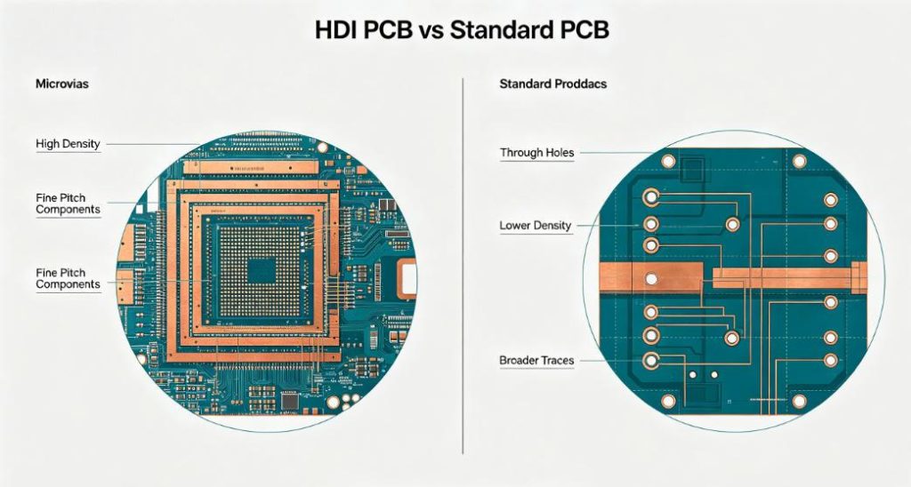
What Exactly Is an HDI PCB?
Let’s start with a definition that’s precise rather than marketing-speak.
An HDI PCB is a printed circuit board that uses microvias (laser-drilled holes typically ≤ 0.15 mm in diameter), fine line widths and spacings (down to 50 µm / 50 µm), and thinner dielectric layers to achieve significantly higher wiring density than conventional multilayer boards. Most HDI boards also employ blind and buried vias — vias that connect specific layers without passing through the entire board — rather than relying solely on through-hole vias.
That definition matters because it separates HDI from a few common misconceptions:
HDI ≠ simply adding more layers. A 12-layer conventional board isn’t HDI. It’s just a thick conventional board. HDI is about how layers are connected and how much routing density you pack into each layer.
HDI ≠ ultra-thin PCB. A 0.4 mm board can be conventional. Thickness alone doesn’t define HDI.
HDI ≠ flex PCB. While HDI boards can be thin and sometimes incorporated into rigid-flex designs, the two technologies are orthogonal.
The Quick Comparison
| Parameter | Conventional Multilayer | HDI PCB |
|---|---|---|
| Minimum hole diameter | ≥ 0.3 mm | ≤ 0.15 mm (laser-drilled) |
| Minimum trace width/spacing | ≥ 100 µm / 100 µm | 50 µm / 50 µm or finer |
| Via type | Through-hole (mostly) | Blind, buried, stacked, staggered microvias |
| Typical dielectric per layer | 0.1 – 0.2 mm | 0.05 – 0.1 mm |
| Pad diameter (minimum) | ≥ 0.6 mm | ≥ 0.35 mm |
| Typical pin density | < 100 pins/in² | ≥ 120 pins/in² |
| Drilling method | Mechanical (CNC) | CO₂ or UV laser |
The bottom line: HDI gives you more routing in less space, through fundamentally different via structures and tighter geometry.
The Foundation: Microvia Technology
Everything about HDI flows from one key enabling technology: the microvia.
What Is a Microvia?
A microvia is a laser-drilled blind hole with a diameter of 0.15 mm (6 mil) or smaller and a depth-to-diameter ratio typically at or below 1:1. Unlike a mechanical through-hole that passes through the entire board, a microvia connects just one layer to its neighbor.
Why does that matter? Because when you drill through every layer, you consume routing channels on every layer and force your signal to take the full board thickness even if it only needs to jump one layer. Microvias eliminate that waste. A signal that needs to go from layer 1 to layer 2 does exactly that — no extra parasitic inductance, no unnecessary space consumption.
How Microvias Are Made
Microvias are drilled with either a CO₂ laser (wavelength ~10.6 µm) or a UV laser (wavelength 355 nm). The choice depends on the dielectric material and the target hole size:
- CO₂ lasers are more common and cost-effective. They work well with standard FR4-based dielectrics and can drill holes down to about 75–100 µm reliably. The laser vaporizes the resin and fiberglass, stopping precisely at the copper target pad below.
- UV lasers can achieve smaller holes (down to ~25 µm) and handle a wider range of materials, including those with high glass content. They’re used in the most demanding HDI applications but come with slower throughput and higher equipment cost.
After drilling, the microvia undergoes desmear (cleaning resin residue from the bottom copper pad) and then plating — typically electroless copper followed by electrolytic copper to fill or conformally plate the hole. Filled and plated microvias (also called “filled vias”) are critical for stacked-via structures because they provide a flat copper surface for the next layer’s microvia to land on.
Three Core Microvia Types
Not all microvias are used the same way. Understanding these three structures is essential:
Blind via — Connects one or more outer layers to inner layers, opening on the surface but not on the opposite side of the board. This is the most common microvia structure. On a 6-layer HDI board, for example, layer 1 connects to layer 2 via a microvia, and layer 5 connects to layer 6 the same way. Layers in between are accessed through different mechanisms.
Buried via — Connects inner layers to each other without opening on any external surface. It’s completely hidden inside the board. Buried vias are typically formed by drilling and plating a sub-laminate before the final lamination cycle. They’re common in Type-II and Type-III HDI architectures.
Stacked vs. Staggered microvias — When multiple microvias stack directly on top of each other (connecting layer 1 to 2, then 2 to 3 in a straight column), that’s a stacked via. It saves space but demands perfect fill-and-plate execution and rigorous reliability testing. Staggered microvias offset each layer’s microvia by a minimum distance, trading a little routing space for significantly better reliability and yield. Most production boards use staggered unless the design absolutely demands stacked.
The Four HDI Architecture Types
The IPC standards (IPC-2226 and IPC-2315) define four categories of HDI boards based on via complexity. Understanding these types helps you match your design requirements to the right build — and the right cost tier.
Type I (1+N+1)
The simplest HDI structure. “1+N+1” means one microvia layer on each side of a conventional multilayer core (the N). You get blind vias connecting the outer layers to their adjacent inner layers, but layers in between still rely on through-holes or are connected via the core.
Typical layer count: 4 to 6
Best for: Consumer electronics with moderate BGA pitch (0.65 mm), designs where through-hole vias handle most of the inner-layer routing and you just need better fan-out on the outer layers.
Cost premium over conventional: ~1.2–1.5×
Example: Entry-level smartphone sensor boards, USB-C hub controllers, compact IoT gateway modules.
Type II (1+N+1 with buried vias)
Same as Type I, but adds buried vias within the core. This means inner layers can communicate with each other without going through the board, which frees up significant routing space.
Typical layer count: 6 to 8
Best for: Designs with BGA packages at 0.5 mm pitch that require inner-layer interconnections without adding layers.
Cost premium over conventional: ~1.5–2×
Example: Mid-range smartwatch motherboards, automotive ADAS camera modules.
Type III (2+N+2)
Now you have two microvia layers on each side of the core. This allows stacked or staggered microvias spanning multiple outer layers and gives you dramatically more routing density.
Typical layer count: 8 to 12
Best for: High-end smartphones, tablets, and networking equipment with fine-pitch BGAs (≤ 0.4 mm), DDR4/DDR5 memory interfaces, and dense SoC packages.
Cost premium over conventional: ~2–3×
Example: Flagship smartphone main boards, high-performance edge computing modules, advanced audio processors.
Type IV — Any-Layer HDI (ELIC)
“Every Layer Interconnect.” Every layer pair has its own microvia capability, and vias can span any combination of layers across the entire board thickness. This is the most flexible and dense architecture available.
Typical layer count: 6 to 16+
Best for: Ultra-dense designs with multiple fine-pitch BGAs, high-frequency RF, and applications where every square millimeter of board area matters.
Cost premium over conventional: ~3–5×
Example: Premium smartphone motherboards (flagship devices), aerospace sensor arrays, cutting-edge medical imaging systems.
| Architecture | Microvia Layers | Buried Vias | Typical Layers | Relative Cost | Best BGA Pitch |
|---|---|---|---|---|---|
| Type I | 1+1 | No | 4–6 | 1.2–1.5× | ≥ 0.65 mm |
| Type II | 1+1 | Yes | 6–8 | 1.5–2× | ≥ 0.5 mm |
| Type III | 2+2 | Yes | 8–12 | 2–3× | ≥ 0.4 mm |
| Type IV (ELIC) | All | Optional | 6–16+ | 3–5× | ≤ 0.35 mm |
A note on cost: The multipliers above are rough guidelines. Actual pricing depends heavily on volume, panel utilization, layer count, copper weight, surface finish, and your chosen supplier’s capabilities. At high volumes (10k+), the per-unit premium narrows considerably because HDI often enables layer count reduction — a Type-III 8-layer board might replace a conventional 14-layer board, saving material and lamination cycles even with the added microvia processing.
The Real Advantages of HDI PCBs
Now we’ve covered the what and the how. Let’s talk about why you’d actually want to go through the trouble.
1. Dramatic Size Reduction
This is the headline advantage, and it’s not incremental — it’s transformational.
Because microvias are 5–10× smaller than mechanical through-holes, the pads and keep-out zones around them shrink proportionally. That frees up routing channels on every layer. Finer trace widths and spacings add even more capacity. The net result: the same circuit on an HDI board typically takes 30%–50% less area than on a conventional multilayer.
The flip side is equally valuable. For a fixed board size, HDI lets you pack more functionality — more components, more signal lines, more power and ground connections — without adding layers.
Real-world example: A flagship smartphone manufacturer reduced their main board from 12 conventional layers to 8 HDI layers while maintaining identical routing density, reducing board thickness by 0.4 mm — critical space for a larger battery.
2. Superior Signal Integrity
This advantage is often underestimated by engineers who focus only on miniaturization.
Shorter, more direct signal paths translate directly into better electrical performance:
- Reduced parasitic inductance: A through-hole via passing through 8 layers adds roughly 1–2 nH of inductance. A microvia connecting two adjacent layers adds roughly 0.1–0.3 nH — an order of magnitude improvement. At multi-gigahertz frequencies, that difference shows up clearly on an eye diagram.
- Lower crosstalk: Thinner dielectric layers between signal and reference planes keep return currents tightly coupled, reducing electromagnetic coupling between adjacent traces.
- Improved impedance control: Thinner, more uniform dielectric layers make it easier to maintain tight impedance tolerances across long traces — critical for DDR5 memory interfaces and high-speed serial links like PCIe Gen 5.
- Reduced EMI: Shorter vias and shorter traces mean less antenna effect, less radiation, and fewer compliance issues during EMC testing.
For any design operating above 3 GHz or with multi-gigabit serial interfaces, HDI isn’t just a convenience — it can be a requirement for meeting signal integrity specifications.
3. Better Thermal Management
HDI boards handle heat better than conventional boards, even without dedicated thermal management strategies, for two reasons:
Thinner dielectrics reduce thermal resistance. Heat generated by a component on the top layer needs to travel through the dielectric to reach inner copper planes or the bottom side. In a conventional board, that dielectric might be 0.2 mm thick per layer. In an HDI board, it’s 0.05–0.1 mm — cutting the thermal resistance path by half or more.
Filled microvias act as thermal vias. A copper-filled microvia is a direct copper highway from one layer to the next. When you place a cluster of them under a thermal pad — which is common practice in HDI designs — you create an efficient vertical heat conduction path that’s far superior to a few scattered through-hole vias.
Real-world example: A power management IC package on an HDI board runs 8–12°C cooler than the same IC on a conventional 4-layer board, solely from the reduced dielectric thickness and microvia thermal paths. That might not sound like much, but it often translates to a 15%–20% improvement in expected lifetime for electrolytic capacitors nearby.
4. Design Freedom
HDI fundamentally changes what’s possible in board layout:
Layer count reduction. This one is counterintuitive but important. By packing more routing per layer, HDI often allows you to meet your design requirements with fewer total layers. A 6-layer HDI board can sometimes replace an 8-layer or even 10-layer conventional board, saving material cost and lamination complexity.
BGA fan-out becomes straightforward. For fine-pitch BGAs (0.4 mm and below), conventional through-hole fan-out often requires multiple signal layers just for escape routing. HDI’s microvias let you fan out directly from the BGA pad to adjacent layers, dramatically simplifying what used to be a layout nightmare.
Flexible power and ground plane design. With buried vias, inner power and ground planes can be segmented and connected without surface-level via congestion, giving you cleaner power distribution and better plane integrity for controlled-impedance signals.
5. Weight Reduction
For most consumer electronics, a few grams don’t matter. But in aerospace, satellite, and wearable applications, every gram counts.
HDI contributes to weight reduction through:
- Fewer layers (less copper and dielectric material)
- Thinner overall board thickness
- Smaller board area (less total material)
A satellite communication module redesigned from 10-layer conventional to 8-layer ELIC HDI achieved a 22% weight reduction — meaningful when you’re paying $20,000+ per kilogram to reach orbit.
The Honest Part: HDI Costs and Limitations
No technology guide is complete without an honest discussion of the downsides. HDI is powerful, but it’s not free, and it’s not always the right answer.
Cost
Let’s not sugarcoat this: HDI costs more per unit area than conventional PCB manufacturing. The reasons are straightforward:
- Laser drilling equipment is expensive to purchase and maintain
- Fill-and-plate processing adds steps and cycle time
- Multiple sequential lamination cycles for Type III/IV boards increase handling and reduce yield
- Tighter tolerances require more inspection and testing
How much more? For low volumes (< 100 panels), expect 2–3× the cost of a comparable conventional board. For high-volume production (> 10,000 panels), the premium narrows to 1.5–2× — and can approach cost parity if HDI enables you to drop 4+ layers.
When does the math work? When the value of smaller size, better performance, or fewer layers exceeds the manufacturing premium. In consumer electronics, where a few square centimeters of saved board area can mean a thinner product or a larger battery, the ROI is usually obvious. In cost-sensitive industrial or commodity applications, it’s often not.
Design Complexity
HDI design rules are more demanding:
- Microvia pad and anti-pad sizes must be precisely defined for your chosen supplier
- Stacked vias require specific drill-depth and fill specifications
- Layer symmetry in the stackup is critical for warpage control — more layers and more asymmetric via structures make this harder
- Impedance calculations become more involved with thinner, variable dielectric layers
If your design team hasn’t worked with HDI before, budget time for learning or bring in experienced support.
Manufacturing Availability
Not every PCB fabricator can make HDI boards. Laser drilling equipment, sequential lamination capabilities, and fill-and-plate processes are significant capital investments. You’ll find HDI capability concentrated among mid-to-high-tier manufacturers, particularly in Asia. This isn’t a barrier for most companies, but it’s worth confirming early — especially if you have supplier constraints or need domestic manufacturing.
Repairability
Once a microvia fails — whether from thermal cycling fatigue, manufacturing defect, or physical stress — repair is extremely difficult. Through-hole vias can sometimes be repaired by manual rework. Stacked microvias buried under three layers of copper and dielectric? Not so much.
This means HDI designs demand more rigorous reliability testing upfront: thermal cycling (IPC-SM-785), mechanical bend testing, and electrical continuity monitoring on microvia chains.
When Should You Choose HDI? A Decision Framework
You don’t need HDI just because it exists. Here’s a practical framework:
Choose HDI when:
- Your BGA pitch is ≤ 0.5 mm — at this spacing, through-hole fan-out becomes impractical or impossible without excessive layer counts
- Board space is severely constrained and the functional density demands it
- Your design operates above 3 GHz and signal integrity is critical
- You need to minimize layer count while maintaining high routing density
- Weight reduction is a hard requirement (aerospace, wearables)
- The product is in a competitive consumer segment where size is a differentiator
Reconsider HDI when:
- BGA pitch is ≥ 0.65 mm and your routing fits comfortably on a conventional stackup
- Board area is not a constraint
- Operating frequencies are low (< 1 GHz) and signal integrity requirements are modest
- The product is cost-sensitive and in high volume where every cent per unit matters
- Your manufacturer doesn’t have proven HDI capability at the type you need
Start with a feasibility check
If you’re on the fence, run a quick comparison: design the same circuit conventionally and in HDI, compare layer counts, board area, and estimated cost. The numbers will usually make the decision obvious.
Real-World Applications
Flagship Smartphones
This is HDI’s flagship application (pun intended). A modern smartphone main board is typically Type-III HDI with 8–10 layers, packing a SoC with 0.35 mm ball pitch, LPDDR5 memory, multiple RF transceivers, power management ICs, and a dozen sensors onto a board roughly 40 mm × 80 mm.
Without HDI, achieving this density would require 14–16 conventional layers — making the board too thick for the enclosure and too heavy for comfortable handling. HDI made it possible to deliver desktop-class computing power in something that slips into your pocket.
Medical Endoscope Camera Modules
A modern endoscope camera head is roughly 6 mm in diameter. Inside it, a Type-IV ELIC HDI board integrates a CMOS image sensor, LED driver circuit, video compression IC, and a connector interface — all on a board smaller than a fingernail.
Before HDI, this required three separate PCBs connected by flex cables, adding failure points and increasing the assembly’s outer diameter. The HDI redesign reduced it to a single board, improving reliability and enabling a slimmer, less invasive instrument.
Automotive LiDAR Systems
LiDAR sensors for autonomous driving and ADAS contain dense arrays of photodetectors, analog front-end circuits, and high-speed digital processing on a very compact module. The difference in resolution between two adjacent detector channels can be 0.1 mm — requiring differential pair routing at tight spacing across a board that also carries significant power.
HDI (typically Type II or III) provides the combination of fine routing density, controlled impedance, and thermal performance needed to make these modules work reliably in the harsh automotive environment (−40°C to +125°C ambient, constant vibration).
Five Key Considerations When Designing an HDI Board
If you’ve decided HDI is the right path, here are five areas where early attention saves headaches later:
1. Define your via structure and stackup early. The choice between stacked and staggered microvias, the number of microvia layers, and the position of buried vias all need to be locked in before layout begins. Changing these mid-project means redesigning the stackup and potentially your entire routing plan. Get your manufacturer’s input on what they can reliably build.
2. Understand the fill-and-plate process. If you’re using stacked microvias, every microvia in the stack must be filled and plated flat before the next layer is laminated. This is a critical process step — incomplete fill creates voids that become reliability failures under thermal cycling. Ask your supplier about their fill process and reliability test results.
3. Control dielectric thickness carefully. HDI dielectric layers are thin, and thin layers have proportionally larger impact from manufacturing variation. A ±10% tolerance on a 0.05 mm dielectric is ±5 µm — tight, but achievable with good process control. Specify your tolerance requirements and ask your supplier what they can hold.
4. Plan your reliability testing program. Microvia reliability is well-proven in the industry, but only when the manufacturing process is properly controlled. Your test plan should include: thermal cycling (at least 1,000 cycles per IPC-9701), microvia chain continuity testing (resistance increase < 10%), and cross-section analysis on first-article boards.
5. Engage your manufacturer early. This can’t be overstated. HDI designs benefit enormously from early collaboration with the fabricator. They can tell you which via structures they build reliably, what their minimum annular ring is, whether they recommend filled or conformal plating, and what their lead time looks like. This input, received before layout starts, can save you a redesign cycle.
Frequently Asked Questions
“Can HDI reduce my layer count?”
Often, yes. A common example: replacing a 12-layer conventional board with an 8-layer Type-III HDI board. The exact savings depends on your routing density and signal requirements, but 30%–40% layer reduction is realistic for dense designs. Run both stackups through an impedance and routing tool to confirm.
“Is any-layer HDI worth the premium over Type III?”
It depends on your BGA density and how many unique signal layers each BGA needs to access. If most of your fine-pitch BGAs fan out from the outer layers and only a few inner-layer connections are needed, Type III with buried vias is probably sufficient. If you have multiple BGAs requiring inner-layer fan-out across different layer pairs, ELIC eliminates complex via-in-pad breakout schemes and is often worth the cost.
“Why do some HDI boards actually have higher yield than conventional boards?”
It sounds counterintuitive, but the mechanism is simple: HDI’s smaller vias and finer traces are laser-drilled and laser-defined, which are inherently more precise than mechanical drilling. Mechanical drill bits wear, wander, and break more often at small diameters. Laser drilling doesn’t. For very dense designs, HDI can actually produce fewer defects per panel than trying to achieve the same routing with conventional tools pushed to their limits.
“My PCB supplier says they can’t do HDI. What are my options?”
You have three: find a supplier with HDI capability (there are many, particularly in China’s Guangdong and Jiangsu provinces, as well as in Japan, South Korea, and Taiwan), relax your density requirements to fit conventional manufacturing, or consider whether a clever redesign with different BGA selections could eliminate the HDI requirement entirely.
“What’s the minimum order quantity for HDI boards?”
Most HDI-capable suppliers accept prototype quantities (5–20 pieces), but pricing per unit will be significantly higher at low volumes. For cost-effective HDI production, volumes above 500–1,000 panels are where the economics start to make sense.
Conclusion
HDI PCB technology isn’t a luxury or a marketing gimmick — it’s a practical, well-established solution to the very real challenge of packing more electronics into smaller spaces while maintaining (or improving) signal integrity and reliability.
It’s also not a one-size-fits-all answer. The cost premium is real, the design complexity is higher, and the manufacturing requirements are more demanding. The right call is to evaluate HDI against your specific requirements — board size constraints, BGA density, signal frequencies, thermal loads, budget, and production volume — and make a data-driven decision.
If your design has fine-pitch BGAs, high-frequency signals, or aggressive size targets, HDI is likely worth exploring. If you’re building a straightforward industrial controller with standard-pitch components and generous board space, conventional multilayer will probably serve you just fine at a lower cost.
Either way, the decision should be made early — ideally during the schematic and floor-planning phase, before you’ve committed to a stackup. And the single best thing you can do is talk to your PCB manufacturer before you finalize your design rules. Their input on what’s reliably buildable will save you money, time, and frustration.



0 Comments