




In hardware development, this is a nightmare almost every engineer has experienced: a circuit board performs flawlessly in the lab. However, when you confidently send it to the certification lab for FCC Part 15 testing, you are told that it exceeds the limit by 12dB at 200MHz. The project is delayed for two months, mass production plans are stalled, and the team is forced to work overtime to redesign and rework.
Electromagnetic Interference (EMI) is often labeled as “black magic.” In reality, EMI is purely a physical phenomenon. As long as we understand the current flow paths, loop areas, and reference planes in the early stages of design, we can systematically eliminate the vast majority of EMI hazards during the schematic and layout phases. The cost of preventing EMI during the design phase is 10∼100 times lower than fixing it with shielding cans and filters after prototyping.
In this article, we begin by examining the physical origins of electromagnetic interference, outline the most effective PCB layout and routing strategies based on priority, and explore ways to create a “quiet” circuit board right from the initial design stage.
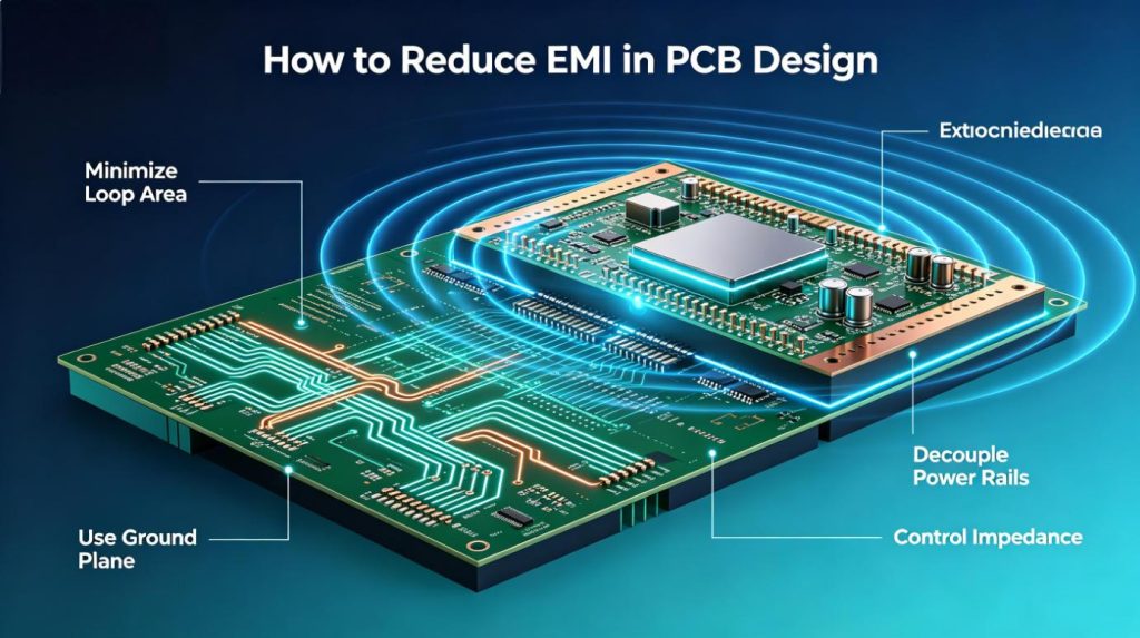
Chapter 1: Understanding EMI on PCBs — Starting from Current Loops
Before discussing how to reduce EMI, we must understand how it is generated on a PCB.
1.1 What is EMI and why is the PCB the main source?
When high-frequency currents flow along PCB traces, these traces and their return paths form closed loops. According to electromagnetic field theory, any changing current loop radiates electromagnetic waves outward. In this case, the trace on the PCB acts as a “loop antenna.”
The radiated electric field strength E can be expressed by the following simplified formula:
Where:
- is the radiated field strength (electric field strength)
- is the frequency of the current (more precisely, the rate of change of the signal edge)
- is the loop area of the current loop
- is the magnitude of the current in the loop
As can be seen from the formula, the higher the frequency , or the larger the loop area , the radiated field strength will increase exponentially or linearly. For a determined chip, it is difficult to change its operating frequency and driving current , so controlling the loop area becomes the most critical means for PCB engineers to reduce EMI.
1.2 Return Path — The First Key to Understanding EMI
To control the loop area, we must first be clear that “current is always a closed loop.” After the current in the signal trace flows to the load, it must return to the power supply or ground (the return source) through some path.
At different frequencies, the return path chosen by the current varies greatly:
- Low-frequency signals (typically below a few hundred kHz): The current will search for the path of minimum resistance to return. Since resistance dominates at low frequencies, the return path will follow the path of minimum resistance (usually the shortest physical straight-line path connecting the source and the load).
- High-frequency signals (typically above a few MHz): At this point, inductive reactance dominates. The high-frequency current will choose the path of minimum inductance to return. Physical laws tell us that when the return current flows closely underneath the signal trace on the reference plane (ground plane or power plane), the loop inductance is minimized.
This means that for high-speed or high-frequency signals, the return current does not take the “shortest straight line,” but flows “like a shadow” along the copper right beneath the signal trace.
1.3 Loop Area — The Direct Determinant of EMI
If there is a complete and continuous reference plane under the signal trace, the distance between the signal trace and the return path is only the dielectric thickness (usually 0.1∼0.2 mm). At this time, because the two are extremely close, the loop area A is extremely small, the magnetic fields cancel each other out, and the outward radiation is almost zero.
Conversely, if the return path is cut (for example, there is a split in the reference plane), the current is forced to detour a long way to get back to the source. This widens the physical distance between the signal trace and the return line, causing the loop area to surge, thereby forming a highly efficient radiating antenna in the air.
Chapter 2: EMI Mitigation Priority — What to Do First
Many engineers, when encountering EMI problems, habitually pile ferrite beads, common-mode chokes, or metal shielding cans directly onto the circuit. This “patching” approach not only increases the Bill of Materials (BOM) cost but also often yields minimal results.
When designing a PCB, we should follow the priority list below, optimizing step-by-step from the underlying physics to the surface-level remedies:
- Priority 1 (Base Physical Layer): Control Return Path and Loop Area
- Ensure reference plane continuity, eliminate split plane crossings, and reduce the current loop area of high-speed signals.
- Priority 2 (System Architecture Layer): Partitioned Layout and Noise Source Isolation
- Physically isolate sensitive analog circuits and high-frequency digital circuits from strong noise sources like switching power supplies.
- Priority 3: Decoupling and Power Distribution Network (PDN) Design
- Place decoupling capacitors reasonably to reduce high-frequency impedance of the power rails, providing a local loop for transient switching currents.
- Priority 4: Routing Constraints and Impedance Control
- Optimize the geometric structure of high-frequency traces, and control crosstalk, edge rates, and board edge radiation.
- Priority 5 (Last-Line Remedies): Filters, Ferrite Beads, and Shielding
- Use common-mode chokes and filters at interfaces, or install shielding cans in locally sensitive areas for final electromagnetic containment.
Chapter 3: Priority 1 — Controlling Return Paths and Loop Areas
3.1 Ensure every high-speed signal has a continuous reference plane
During stack-up design, you must ensure that the layer adjacent to all high-speed signal traces (such as clocks, high-frequency data lines, and differential pairs) is a complete and continuous ground plane (GND) or power plane (PWR). For multi-layer boards, an alternating structure of “Signal-GND-Signal/PWR-GND” is highly recommended so that every signal layer is tightly coupled to a reference plane.
3.2 Never cross split reference planes
In mixed-signal boards, engineers sometimes split the ground plane (for example, separating analog ground AGND from digital ground DGND, or splitting power planes of different voltages).
If high-speed signal traces cross these split lines, the return current will be forced to detour around the edges of the split.
This not only causes severe signal reflections due to impedance discontinuity but also leads to a surge in the loop area, which can increase the radiation intensity at the split crossing by 10∼20dB.
3.3 How to remedy if crossing a split is unavoidable?
In rare cases where crossing a split is completely unavoidable, stitching capacitors must be used:
- Place a low-impedance capacitor (typically 10 nF∼100 nF) directly over or as close as possible to the signal crossing point, connecting the two sides of the split.
- This capacitor provides a high-frequency “bridge” for the return current, thereby limiting the loop area.
- A better practice is to replan the routing or component layout to completely avoid crossing splits.
📝 Case Study: DDR3 Clock Trace Crossing a Split Plane Leading to EMI Failure
During the development of an industrial control board, the differential clock lines running at 800 MHz between the CPU and DDR3 memory chips were routed. Due to routing space constraints, the layout engineer routed this clock pair on the bottom layer, which accidentally crossed a split line between the internal 1.5 V (DDR power) and 3.3 V (I/O power) planes. Additionally, the adjacent ground plane had a local cutout near the transition vias.
- Observation: During 3-meter anechoic chamber testing, the product exhibited sharp narrow-band radiation spikes at 800 MHz and its harmonic 1.6 GHz, exceeding the FCC Part 15 Class A limit by 14 dB.
- Root Cause Analysis: The high-frequency return current at 800 MHz could not cross the split in the power plane or the ground plane cutout. The return current was forced to detour to decoupling capacitor vias and ground vias located 12 mm away to return. This increased the transient return loop area by dozens of times. According to , this large loop acted as a highly efficient dipole antenna at 800 MHz.
- Resolution: The DDR3 routing area was redesigned. The clock lines were rerouted to Layer 3, which was adjacent to a continuous ground plane, ensuring no splits or large via cutouts existed underneath their routing path. After rebuilding the prototype, the radiation at these frequencies dropped by 18 dB, successfully passing the certification.
3.4 Return paths of differential pairs
A common misconception is: “Differential signals act as each other’s return path, so they don’t need a complete ground plane.”
In reality, differential traces cancel each other’s fields perfectly only under ideal, perfectly symmetrical conditions with zero common-mode noise. In the real world, any trace asymmetry or propagation skew from the transmitter will generate common-mode currents. These common-mode currents must return through the nearest ground plane. Therefore, differential pairs also need to run close to a continuous reference plane and must not cross splits.
3.5 Special treatment for crystal oscillators and clock sources
Clock signals are the primary radiation sources on a PCB, with energy concentrated at their fundamental frequency and high-order harmonics.
- Never route clock traces across split planes.
- Do not route any other signal traces under the crystal oscillator. In multi-layer boards, a Ground Island should be placed on the copper layers directly beneath the crystal oscillator, stitched directly to the main ground plane using multiple vias.
- You can apply “Guard Traces” (ground shielding) on both sides of the clock trace. The guard traces should be connected to the ground plane with vias spaced every (one-twentieth of the wavelength) to prevent clock energy from coupling outwards.
Chapter 4: Priority 2 — Layout Isolation and Noise Source Management
The layout phase determines about 80% of a PCB’s EMC performance. Poor routing can be fixed by rerouting, but a bad layout usually requires starting over from scratch.
4.1 Categorizing EMI noise sources and sensitive zones
The circuit should be partitioned into distinct physical areas during layout:
| Zone Category | Representative Components | Radiated Characteristics | Handling Rule |
|---|---|---|---|
| Noise Sources | Switching regulators (DC-DC), motor drivers, power MOSFETs | Very high di/dt and dv/dt | Group together, keep far from chassis ground and external connectors |
| High-Speed Signals | CPU/MCU, DDR memory, clock generators, high-speed interfaces | Continuous high-frequency pulses | Center-align, place close to GND planes, keep traces short |
| Sensitive Analog | ADC front-ends, low-noise amplifiers, precision references | Easily disturbed by external noise | Isolate with clean ground, keep away from noise zones |
| Interface I/O | RJ45, USB, HDMI, power input connectors | Easy to couple noise and radiate via cables | Place at the board edge, apply dedicated filtering |
4.2 DC-DC converter layout essentials
Switching regulators are the largest source of low-frequency electromagnetic radiation (typically ranging from 100 kHz∼30 MHz, with high-order harmonics extending above 100 MHz) on a board. The core of DC-DC EMI optimization is minimizing the Hot Loop area.
The loop where current undergoes rapid changes (high di/dt) during the turn-on and turn-off of switching transistors is called the hot loop. According to Maxwell’s equations, rapid current changes generate induced electromotive force through stray inductance:
If (caused by excessively long traces) is large, it will excite high-frequency voltage spikes and ringing at the switch node (SW), generating strong electric field radiation.
📝 Case Study: Large Input Capacitor Loop of Synchronous Buck Regulator Causes High-Frequency Noise
An automotive infotainment device contained a 12 V to 3.3 V / 3 A synchronous buck regulator running at 2.2 MHz in a QFN package.
- Observation: During CISPR 25 Class 3 Conducted Emission (CE) testing, the device showed severe broadband noise exceeding the limit by 8 dBμV in the 110 MHz∼160 MHz frequency band.
- Root Cause Analysis: Probing the SW switch node with an oscilloscope revealed high-frequency ringing with a peak-to-peak voltage of 5.5 V at a frequency of approximately 135 MHz riding on the rising edge of the switching waveform. Inspection of the PCB layout showed that the 10\muF ceramic input decoupling capacitor was placed 6 mm away from the chip’s pin due to feedback routing bottlenecks, and connected with a thin 15 mil trace. This trace introduced approximately 4 nH of stray inductance . When the internal MOSFET switched in 4 ns, the high excited strong resonance.
- Resolution: The layout was modified to use an 0603 size input decoupling capacitor placed directly adjacent to the and PGND pins of the IC, using a wide 60 mil copper shape to connect them. This reduced the physical distance to under 0.8 mm. Retesting showed the SW node ringing dropped below 1.2 V, and the noise in the 110 MHz∼160 MHz band decreased by 15 dBμV, passing the CISPR 25 test.
4.3 Interface and cable radiation control
Even if a PCB itself has very low radiation, it can easily fail EMI tests once external cables (such as USB cables or power cords) are plugged in. This happens because common-mode currents on the board couple onto the cables, turning the cables into radiating antennas.
- I/O Filtering: Place common-mode chokes or filter capacitors immediately next to the pins of all external connectors.
- Chassis Ground vs. Signal Ground Isolation: The ground at the connector interface (Shield GND/Chassis GND) should be physically isolated from the internal system signal ground (Signal GND). They should only be bridged via high-voltage capacitors or a single point (such as a ferrite bead) to prevent internal noise currents from flowing onto the outer shield of the cable.
Chapter 5: Priority 3 — Decoupling and Power Distribution Network (PDN)
When digital ICs operate, their internal transistors switch state simultaneously, drawing high transient currents from the power rail. If the power distribution system cannot respond immediately, it will cause voltage ripples (power noise) on the power rails, which will propagate and radiate through the power network.
5.1 The true nature of decoupling capacitors
Decoupling capacitors do not simply “filter” noise; they act as a local, low-impedance reservoir to supply transient switching currents to the chip.
If the decoupling capacitor is placed too far from the chip, the transient current must travel through longer traces and vias. The parasitic inductance of these traces will restrict the fast delivery of current, resulting in transient voltage droop at the chip pins and radiating electromagnetic noise over a larger loop.
5.2 Location is more important than capacitance value
When designing decoupling networks, placement and via layout are critical:
- The closer, the better: Decoupling capacitors must be placed as close as possible to the power pins of the chip.
- Minimize pin inductance: Traces connecting the capacitor pads to the chip pins should be short and wide. Vias should be placed directly to the side of the capacitor pads rather than at the end of a long, thin trace, as vias themselves introduce about 0.5∼1 nH of parasitic inductance.
5.3 Plane-to-plane capacitance of power and ground layers
In high-speed multi-layer board design, placing the power plane and the ground plane on adjacent layers with a dielectric thickness of less than 0.1 mm (e.g., 2 mil∼3 mil) yields a high plane-to-plane capacitance. This natural capacitor exhibits extremely low impedance at high frequencies (above 100 MHz∼1 GHz), providing decoupling performance that far exceeds discrete surface-mount capacitors.
Chapter 6: Priority 4 — Routing Constraints and Impedance Control
Once the physical layout and return paths are established, we can fine-tune our routing rules to further optimize signal integrity and reduce radiation.
6.1 High-speed routing and via management
- Minimize the number of vias on high-speed signal lines. Each via introduces an impedance discontinuity. If there is no nearby transition ground via, the return current will be forced to detour when the signal changes layers.
- Transition via placement: When a high-speed signal transitions from Layer 1 to Layer 3, a ground via must be placed within 1 mm of the signal transition via to allow the return current to transition seamlessly between the two reference ground planes.
6.2 Suppressing crosstalk: The 3W Rule
When two traces run too close together, their electromagnetic fields couple to each other, generating crosstalk.
- The 3W Rule: The center-to-center spacing between two adjacent traces should be at least 3 times the width of the trace (i.e., the air gap between trace edges is at least 2W). This reduces the electromagnetic coupling between the traces by about 70%.
- The 5W Rule: For highly sensitive traces like clock lines or differential pairs, it is recommended to expand the spacing to 5 times the trace width.
6.3 Edge rate control (Rise time control)
The radiation capability of a signal is highly dependent on its rise time. Steeper rising edges contain richer high-frequency harmonic components, resulting in a wider radiation spectrum.
- Without violating setup times, you can place a small series termination resistor (typically 10∼33 Ω) at the driver’s output.
- This resistor works with the parasitic capacitance of the trace to form a low-pass filter, slowing down the rising edge, absorbing high-frequency reflections, and lowering high-frequency radiation.
6.4 Board edge radiation control (20H rule and via shielding)
Due to electromagnetic boundary effects, the electromagnetic fields between the power and ground planes tend to leak outward at the board edges.
- The 20H Rule: Retract the power plane relative to the ground plane by 20H, where H is the dielectric thickness between the two planes. This can reduce edge radiation by about 70%.
- Via Shielding: Placing a row of stitching ground vias along the board edge with a spacing of less than (typically 1∼2 mm) creates a Faraday cage, effectively blocking internal electromagnetic waves from leaking out of the board sides.
Chapter 7: Priority 5 — Filters, Ferrite Beads, and Shielding (Last-Line Remedies)
When we have addressed layout, return paths, and decoupling, the board’s electromagnetic radiation is usually well below the limit. At this point, the fifth priority—filters, ferrite beads, and physical shielding—acts as the final defense line, primarily resolving residual issues related to external cable coupling and direct spatial radiation.
7.1 Common-mode choke and filter design
External cables are the most vulnerable parts of a PCB system to forming dipole antennas. To prevent high-frequency common-mode noise from flowing onto the cables, a filter barrier must be placed right at the physical interface.
- Common-Mode Chokes: Differential signals (such as USB, HDMI, and Ethernet) carry useful information in differential mode, while interference noise is typically common-mode. A common-mode choke exhibits very low impedance to differential-mode signals but presents high impedance to common-mode noise, preventing common-mode currents from flowing out of the board.
- Filter Topology Selection: Choose the appropriate filter network based on the source and load impedance:
- Use a T-filter if both sides are low-impedance.
- Use a π-filter if both sides are high-impedance.
- Use an L-filter or reversed L-filter if one side is high and the other is low.
7.2 Selection rules for ferrite beads
A ferrite bead is a resistive component whose impedance changes with frequency. Its equivalent impedance Z is determined by its inductive reactance and resistance :
At low frequencies, the bead is inductive (X dominates), reflecting noise. At high frequencies (usually between 30 MHz∼1 GHz), its resistive component R spikes, converting high-frequency noise into heat. When selecting a bead, ensure that the target noise frequency lies within the bead’s resistive operating region.
7.3 Metal shielding cans and slot leakage
Metal shielding cans are used to block spatial radiation. When high-speed CPUs, RF front-ends, or sensitive analog amplifiers cannot be resolved by routing, a shielding can is necessary.
- Control of Slot Leakage: The spacing between grounding pins/solder pads (d) of the shielding can must be much smaller than the wavelength of the noise. Generally:
If the spacing is too large, the gap will act as a slot antenna, letting high-frequency electromagnetic waves leak out.
📝 Case Study: USB 2.0 Interface Lacking Common-Mode Choke Leads to Cable Radiation Failure
In a medical monitor project, the on-board MCU transmitted data to an external display terminal via a USB 2.0 interface (operating at 480 Mbps with a fundamental clock frequency of 240 MHz).
- Observation: During Radiated Emission (RE) testing in a 3-meter anechoic chamber, plugging in the USB cable caused massive vertical polarization radiation spikes at 240MHz, 480MHz, and 720MHz, exceeding the limit by 16dB. Unplugging the USB cable eliminated the spikes completely.
- Root Cause Analysis: Near-field probing showed that common-mode noise coupled from the internal digital power rails was present on the USB D+ and D− differential lines. To save BOM cost, the original design only included ESD protection diodes on the D+/D− lines without a common-mode choke. The common-mode current traveled down the USB cable, making the cable shield and conductors act as a radiating antenna at 240MHz and its harmonics.
- Resolution:
- A common-mode choke with an impedance of 90Ω at 100MHz was placed directly next to the USB Type-A connector on the D+/D− lines.
- The metal shield of the USB connector was connected to the system ground (GND) through multiple parallel 100 nF ceramic capacitors, and a ferrite bead was placed in series with the power line. Retesting showed the cable-induced common-mode radiation at 240MHz dropped by 21dB, successfully passing the test.
Chapter 8: Common Misconceptions in EMI Control (What Seems Useful But Isn’t)
In engineering practice, there are several widely circulated “rules of thumb” that lack physical backing. We need to distinguish these from true physical solutions.
8.1 The pros and cons of copper pouring
Misconception: “Pouring copper over all empty spaces of the board and connecting it to ground will always improve EMI.”
- Fact: Copper pours are only effective if they are connected to the low-impedance ground plane with a high density of vias.
- If a large copper area is only grounded through one or two isolated vias, or left floating (referred to as “dead copper”), it will act as a highly efficient patch antenna, severely worsening EMI.
- Advice: Delete any isolated copper fragments that cannot be grounded properly. Grounded copper pours must be stitched to the main ground plane with vias spaced every 1∼2 mm.
8.2 Misuse of ferrite beads
Misconception: “Simply putting a ferrite bead in series on a power line will absorb high-frequency noise.”
- Fact: Ferrite beads act as resistors to consume noise only in specific frequency bands, while remaining inductive at lower frequencies. If poorly matched, the bead’s inductance and the downstream decoupling capacitance can resonate, creating a massive impedance peak at a specific frequency, which actually boosts EMI radiation.
- Advice: You must select the bead model based on the target noise frequency using the impedance curve, ensuring it does not resonate with your decoupling network.
8.3 Over-reliance on shielding cans
Misconception: “We don’t need to worry about EMI during layout; we can just throw a metal shield over it later.”
- Fact: Shielding cans only block spatial radiation; they do nothing to address conducted EMI traveling along traces to external cables. Moreover, shielding cans trap heat, complicate assembly, and increase BOM costs. They should only be used as a final supplement when board-level optimization has been pushed to its limit and minor emission spikes remain.
Chapter 9: EMI Debugging and Testing — Post-Design Strategies
If your PCB has already been manufactured and has failed EMI testing, you can use the following steps to diagnose and resolve the issue.
9.1 Fast localization using near-field probes
Avoid going straight to expensive certification chambers without a plan. You can troubleshoot in your own lab using a portable spectrum analyzer and a set of near-field probes:
- Sweep the board with a magnetic field (H-field) probe to find the areas with the strongest radiation (usually around crystals, DC-DC switch nodes, or interfaces).
- Sweep the edges and cables with an electric field (E-field) probe to check if high-frequency noise is coupling onto power lines or external wires.
9.2 Diagnosing based on the failing frequency
- Below 30 MHz: Typically caused by switching power supplies (conducted emissions). Check the input π-filter, hot loop areas, and BOOT resistors.
- 30 MHz∼200 MHz: Typically caused by switching power supply high-frequency ringing or slow clocks. Check the switch node snubber circuits and clock series termination resistors.
- 200 MHz∼1 GHz: Typically caused by high-speed digital buses (DDR/SDRAM), fast clocks, or traces crossing split planes. Check ground plane continuity, transition ground vias, and decoupling capacitor placement.
- Above 1 GHz: Typically caused by high-speed differential serial buses (PCIe/USB3) or via stubs. Check differential impedance control, via antipad sizing, and consider backdrilling.
Chapter 10: EMI Design Checklist
Before sending your PCB to the manufacturer, run through this checklist to ensure all parameters are optimized:
- Stack-up & Reference: Do all high-speed signal layers sit adjacent to a continuous ground plane?
- Split Plane Crossing: Are there any high-speed lines or clocks crossing split reference planes?
- DC-DC Layout: Is the power loop (input capacitor – switch – ground) minimized in area?
- Clock Management: Is the region under the crystal oscillator clear of other traces and isolated with a local ground island?
- Decoupling Efficiency: Are decoupling capacitors placed immediately adjacent to the IC power pins, with vias routed with short, wide traces?
- Crosstalk Prevention: Is a minimum of 3W spacing maintained between high-speed traces and adjacent lines?
- Edge Radiation: Is the power plane pulled back by 20H from the ground plane, and is there a via shield along the board edge?
- I/O Filtering: Do all external interface connectors have filtering or common-mode rejection devices installed next to their pins?
- Copper Pouring: Are all copper pours stitched to ground using multiple vias, eliminating any floating “dead copper”?
Conclusion
Reducing EMI in PCB design is ultimately a balancing act between controlling return path impedance and limiting current loop areas. By prioritizing clean, continuous return paths, optimizing the physical placement of noisy circuits, and applying proper routing constraints and decoupling techniques, you can eliminate over 90% of EMI issues before the first board is ever fabricated.
Remember: Great engineers control electromagnetic fields during the design phase, while average engineers rely on luck at the certification lab. Integrate these rules into your daily layout routine, and pass your EMC tests on the first run.



1 Comment
5V Power Supply PCB Layout: Decoupling, Return Paths and Review Checks - thindry pcb manufacturer · 08/25/2026 at 07:29
[…] These practices support lower coupling risk, but they do not prove EMC compliance. For broader board-level controls, see our guide on how to reduce EMI in PCB design. […]