




A practical guide for engineers, buyers, and anyone who needs to know which PCB testing method actually fits their situation.
Why PCB Testing Deserves More Attention Than It Gets
Most people obsess over PCB design and component sourcing, then treat testing as an afterthought. That’s a mistake that shows up later — usually in the form of field returns, customer complaints, or a costly recall.
The hard truth is that a defect caught on the production line costs a fraction of what the same defect costs when a customer finds it. Industry data consistently puts that multiplier somewhere between 10x and 1,000x depending on the product and market. For medical, automotive, or industrial applications, the consequences go beyond money.
The other hard truth is that there’s no single test method that catches everything. AOI, Flying Probe, ICT, and Functional Testing each cover different failure modes, operate at different cost points, and suit different production volumes. Understanding where each one fits — and where it falls short — is what separates a solid test strategy from a false sense of security.
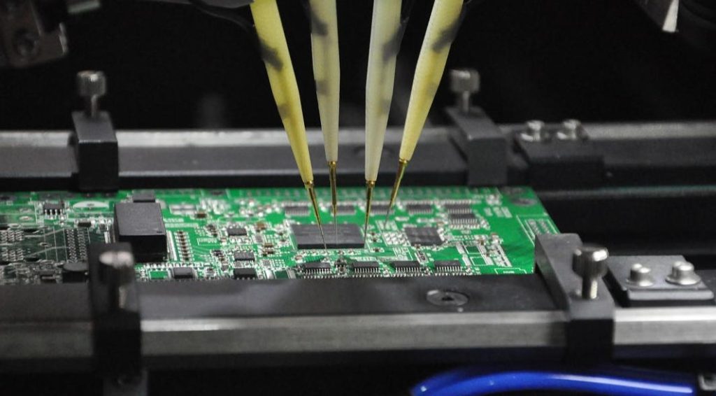
How to Test a PCB Board? This article introduces four common PCB testing methods, featuring real cost data, an honest analysis of limitations, and a practical decision-making framework.
The 4 Methods at a Glance
Before going deep, here’s a quick orientation on where each method sits:
| Method | What It Checks | Best For | Cost Level |
|---|---|---|---|
| AOI | Solder quality, placement, missing parts | Post-reflow, any volume | Low–Medium |
| Flying Probe | Electrical continuity, component values | Protypes, low–medium volume | Medium |
| ICT | Full electrical node coverage, parametric values | High-volume production | High (fixture NRE) |
| FFT | Board performs its real-world function | Final validation, all volumes | Varies |
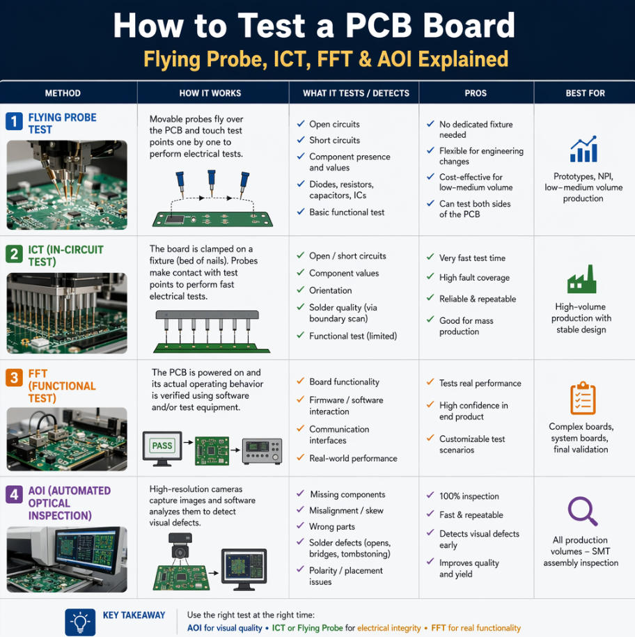
Now let’s get into the detail that actually matters when you’re making a decision.
AOI: Automated Optical Inspection
How It Works
AOI systems use high-resolution cameras — sometimes a combination of 2D and 3D imaging — to photograph every inch of a populated PCB and compare it against a reference program built from your design data or a known-good board. When something doesn’t match, it flags it for review.
What it can catch includes missing components, tombstoning, solder bridges, insufficient solder, wrong polarity on polarized parts, and surface contamination. Modern3D AOI also measures solder paste volume and joint shape, not just whether solder is present.
Where It Fits in the Line
AOI typically sits right after the reflow oven, sometimes after wave soldering as well. Its primary role is process control — catching solder and placement defects while they’re cheap to fix, and flaging process drift before it becomes a yield problem. A sudden spike in AOI alarms is often the first sign that your stencil is clogging or your reflow profile has drifted.
What It Can’t Do
AOI is a camera. It sees surfaces. It cannot detect electrical opens or shorts hiding under a component, it cannot distinguish a 10kΩ resistor from a 100Ω resistor because they look identical, and it cannot see BGA solder joints at all. For those failure modes, you need electrical or X-ray inspection.
False positives are also a real operational burden. If the inspection program is tuned too tightly, your team spends hours re-inspecting boards that are actually fine. Getting the balance right between sensitivity and specificity takes deliberate program engineering and ongoing maintenance.
Cost Reality
Equipment investment runs from around 30,000forabasic2Dsystemupto300,000+ for a high-throughput 3D system. Per-board test time is typically 15–60 seconds. There’s no consumable cost per board, and most contract manufacturers include AOI as part of their standard SMT process — if yours charges a significant premium for it on medium-volume runs, it’s worth a conversation.
Flying Probe Testing
How It Works
Flying probe systems use between 2 and 8 robotic probe arms that physically move across the PCB, touching test points and component pads to make electrical measurements. The test program is generated directly from your Gerber files and netlist, so there’s no custom hardware to build.
The system measures continuity and opens, short circuits, resistance values, capacitance, diode orientation, and some inductance. More advanced flying probe platforms also support basic functional stimulus and JTAG boundary scan.
Where It Belongs
Flying probe is the natural choice for protypes and new product introduction. There’s no fixture to build, so testing can start within hours of receiving design data. For low to medium production volumes — roughly up to a few thousand boards per year on a given design — it often remains the most cost-effective electrical test option. It’s also well-suited to high-mix environments where designs change frequently, because there’s no sunk fixture cost when the BOM gets updated.
The Real Tradeoffs
The main limitation is speed. Testing a single board takes 1–5 minutes depending on node count, compared to 15–30 seconds for ICT. At high volumes, that difference compounds fast. Flying probe also can’t test everything ICT can — some parametric measurements and powered in-circuit tests require the kind of full-board stimulus that a bed-of-nails fixture enables.
Test coverage is also limited to physically accessible test points. Tight-pitch BGAs and hidden vias present real challenges, and the system cannot verify powered functional behavior on its own.
The Break-Even Math vs. ICT
If an ICT fixture costs 8,000inNREandflyingprobetestingruns15 per board at your contract manufacturer, flying probe is cheaper up to roughly533 boards. Beyond that, ICT starts paying back. The exact crossover depends on your test time, labor rates, and how long you expect to run the design — but this is the framework most engineering managers use to make the call.
ICT: In-Circuit Test
How It Works
ICT uses a custom fixture — the classic “bed of nails” — that presses hundreds or thousands of spring-loaded pins simultaneously against dedicated test points on the PCB. The system then applies electrical stimulus across individual nets and measures responses, verifying components and connections across the entire board in one coordinated sequence.
ICT can measure resistor values within tolerance, capacitor and inductor values, transistor and diode behavior, power supply outputs, clock signals, and basic digital logic behavior. Coverage is comprehensive in a way that flying probe simply can’t match at speed.
Where It Belongs
ICT is built for high-volume production. Once the fixture NRE is amortized, the per-board cost drops sharply, and the15–30 second test cycle keeps pace with fast SMT lines. For programs running tens of thousands or hundreds of thousands of boards, ICT is often the only electrical test option that makes economic sense.
The Honest Limitations
The fixture cost is the obvious barrier. A moderately complex board might run 5,000–15,000 in fixture NRE, and that cost resets every time the design changes significantly. For products still in active development, that’s a real risk.
ICT also requires accessible test points designed into the PCB layout. If your layout engineer didn’t leave adequate test point coverage — a common problem when boards get dense — your ICT coverage will have gaps. And like flying probe, standard ICT doesn’t verify real-world functional behavior. It confirms the circuit is built correctly, not that it works correctly under load.
Cost Reality
Fixture NRE: 3,000–20,000 depending on board complexity and node count. Per-board test time: 15–60 seconds. Per-board variable cost is low once the fixture exists — mainly machine time and labor. Equipment ownership costs 100,000–400,000, but most contract manufacturers have ICT capacity as standard service offering.
FFT: Functional Test
How It Works
Functional testing powers up the PCB and exercises it the way it would actually be used in the field. A custom test fixture connects to the board’s I/O — connectors, edge fingers, test points — and a test program sends real signals in and verifies real responses out.
What this means in practice varies completely by product. For a motor controller, it means spinning a motor. For a wireless module, it means transmitting and receiving RF signals and verifying link quality. For a payment terminal, it means running transaction sequences. The test is as specific as the product.
Where It Belongs
Functional testing is typically the last gate before a board is accepted into finished goods. It’s the only method that can catch firmware bugs, wrong firmware versions, RF calibration errors, I/O channel failures, and system-level interactions that no circuit-level test can see.
It works at any production volume, but the economics are different from electrical testing. Because the fixture is essentially a custom piece of test equipment — and because someone has to write and maintain the test software — FFT carries significant upfront engineering cost. For simple, low-volume products, that investment might not be justified. For anything customer-facing or safety-relevant, it almost always is.
What Makes FFT Hard
Writing a functional test that covers all meaningful failure modes requires deep product knowledge and test engineering discipline. Vague functional tests that only check “does it power on and respond” provide false confidence — they pass boards that will fail in specific use conditions. Good functional test coverage is a real engineering deliverable, not something that gets knocked out in an afternoon.
Test fixture maintenance is another ongoing cost. Connectors wear out, cables develop intermittent faults, and the test program needs updating every time firmware or hardware changes. This is real operational overhead that gets underestimated during program planning.
Common PCB Defects and Which Test Catches Them
This is where the rubber meets the road. Here’s an honest map of what each method actually detects across the most common PCB failure modes:
| Defect | AOI | Flying Probe | ICT | FFT |
|---|---|---|---|---|
| Missing component | ✅ Catches | ⚠️ Sometimes | ✅ Catches | ⚠️ Sometimes |
| Wrong component value | ❌ Cannot detect | ✅ Catches | ✅ Catches | ⚠️ Sometimes |
| Solder bridge | ✅ Catches | ✅ Catches | ⚠️ Sometimes | |
| Cold solder joint | ⚠️ Partial | ⚠️ Partial | ⚠️ Partial | ⚠️ Sometimes |
| Open via | ❌ Cannot detect | ✅ Catches | ✅ Catches | ⚠️ Sometimes |
| Wrong polarity | ✅ Catches | ⚠️ Sometimes | ||
| BGA solder void | ❌ Needs X-ray | ❌ Cannot detect | ⚠️ Sometimes | |
| Firmware bug | ❌ Cannot detect | ❌ Cannot detect | ✅ Catches | |
| Wrong firmware version | ❌ Cannot detect | ❌ Cannot detect | ✅ Catches | |
| I/O channel failure | ❌ Cannot detect | ⚠️ Partial | ⚠️ Partial | ✅ Catches |
| RF calibration error | ❌ Cannot detect | ❌ Cannot detect | ✅ Catches |
A few observations worth calling out from this table. Cold solder joints are genuinely hard for every method — they can look fine optically, pass a resistance check at room temperature, and still fail intermittently in the field under thermal stress. This is one reason why thermal cycling and environmental stress screening exist as supplementary methods. BGA solder voids are similarly invisible to anything except X-ray inspection. If you’re using BGAs in a reliability-critical application, X-ray has to be in your process.
How to Build a Testing Strategy That Actually Works
The table above makes one thing clear: no single method covers everything. A realistic test strategy layers methods to build overlapping coverage across different failure categories.
For protypes and NPI, the typical starting point is AOI plus flying probe. AOI catches process defects early and cheaply. Flying probe provides electrical coverage without fixture investment. If the product is complex or safety-relevant, adding a basic functional test at this stage — even a manual one — pays dividends in catching design issues before you’re deep into production tooling.
For medium-volume production (roughly 1,000–20,000 units per year), the decision between flying probe and ICT depends heavily on design stability and fixture amortization math. If the design is stable and volumes are consistent, ICT often makes economic sense. If the design is evolving or volumes are variable, flying probe keeps you flexible. AOI and functional testing remain in the mix regardless.
For high-volume production, ICT is usually the core electrical test. The per-board economics are compelling once fixture NRE is amortized, and the test throughput matches fast production lines. AOI stays in the process for solder quality control. Functional testing handles final acceptance. Some manufacturers add flying probe as a targeted supplement for nodes that the ICT fixture can’t reach.
For any safety-critical or regulatory application, the conversation shifts. Medical devices, automotive electronics, and industrial safety systems often require documented test coverage that goes beyond what production economics alone would drive. In these cases, the question isn’t “what’s the cheapest test strategy” — it’s “what test evidence do we need for regulatory submission and liability management.”
Frequently Asked Questions
Can I test a PCB board at home?
Yes, within limits. A digital multimeter covers basic continuity checks, power supply rail voltages, and component verification. An oscilloscope adds signal integrity visibility. What you can’t replicate at home is the speed, coverage, and statistical power of automated testing — but for hobby projects and debugging individual boards, bench testing with proper instruments gets you a long way.
Which test method has the best ROI?
AOI almost always has the best ROI for any volume above pure hand assembly, because it catches expensive-to-fix defects at the cheapest possible point in the process. For electrical testing, the ROI calculation depends on volume, design stability, and your cost of field failures. There’s no universal answer.
Do I need all four methods?
Probably not all four on every product. Low-volume, low-risk products might only need AOI and flying probe. High-volume consumer electronics typically run AOI plus ICT plus functional test. High-reliability applications add X-ray and may run all four plus environmental stress screening. Match the test investment to the cost of failure in your specific market.
What about X-ray inspection?
X-ray is the fifth major method not covered in depth here. It’s essential for BGA inspection and is increasingly common for press-fit connectors and hidden joint verification. It’s typically a targeted supplement rather than a 100% inspection method, due to throughput and cost constraints.
Closing Thoughts
PCB testing is fundamentally a risk management exercise. Every method in this guide has gaps, and every method has a cost. The goal isn’t to achieve theoretical 100% coverage — it’s to find the combination that catches the failures most likely to hurt your customers and your business, at cost that makes sense for your production economics.
The engineers who build the best test strategies tend to think about it from the failure mode backwards: what are the most likely ways this board can be wrong, what are the consequences of each, and what’s the cheapest point in the process to catch each one? That thinking, more than any specific tool choice, is what separates good test engineering from checkbox compliance.
If you’re evaluating test options for a new program and want to talk through the specifics, the details of your product — volume, complexity, failure consequence, regulatory environment — matter a lot. General frameworks only take you so far.
Please contact us if you have requirements for PCB or PCBA manufacturing and production. Email: [email protected]



0 Comments