




PCB layout is the process of turning an electronic circuit schematic into a physical printed circuit board design. It defines where components sit, how copper traces connect them, where vias and layers are used, how the board fits the product, and what manufacturing files are sent to the PCB factory.
A good PCB layout is not only an attractive drawing. It must satisfy electrical performance, mechanical fit, thermal control, design for manufacturability, design for assembly, inspection access, and testing needs. For buyers, the quality of the layout directly affects prototype success, production cost, lead time, and long-term reliability.
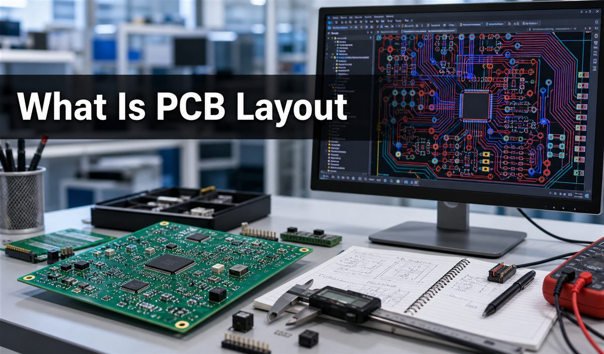
PCB Layout Turns a Schematic into a Manufacturable Board
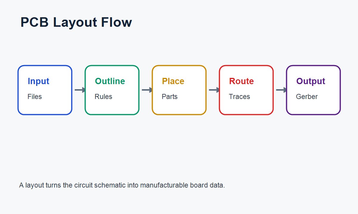
PCB layout converts the logical circuit into physical copper, components, holes, layers, and output files. The schematic says which pins should connect; the layout decides how those connections are built on a real board.
| Related Term | What It Means | When It Applies | Buyer or Engineering Note |
| Schematic | The logical circuit diagram | Before layout starts | Layout must match the schematic netlist. |
| Component placement | Where parts are located on the board | Early layout stage | Placement affects routing, heat, assembly, and test access. |
| Routing | Copper trace and via connections | After placement | Trace width, spacing, layer changes, and return paths matter. |
| Stackup | Layer order, copper, dielectric, and thickness plan | Multilayer and controlled designs | Confirm stackup before routing critical signals. |
| Gerber or ODB++ | Manufacturing output data | Quotation and production | Send the final revision with drill files and notes. |
PCB Layout Is One Part of the Larger PCB Design Process
PCB design includes circuit requirements, component selection, schematic capture, layout, manufacturing review, prototype testing, and revision control. Layout is the part where electrical intent becomes a physical board that a factory can build.
This distinction matters in sourcing. A manufacturer can review layout manufacturability and assembly risks, but it cannot safely guess the circuit intent if the schematic, BOM, or requirements are incomplete. The buyer should keep design files, output files, and revision notes consistent.
Good PCB Layout Starts with Constraints and Component Placement
The best layouts start with board constraints, not with random routing. The designer should define board outline, layer count, connector positions, mounting holes, enclosure limits, current needs, signal classes, impedance needs, thermal areas, and manufacturing rules before routing.
- Fixed mechanical parts: connectors, switches, displays, antennas, sensors, mounting holes, and keep-out areas.
- Critical circuits: clock sources, high-speed interfaces, RF sections, power converters, and sensitive analog areas.
- Thermal parts: regulators, MOSFETs, LEDs, drivers, power resistors, and heat-generating ICs.
- Assembly access: fiducials, test points, polarity marks, programming headers, and rework clearance.
Routing Connects the Circuit While Controlling Electrical Risk
Routing is the layout step that creates copper traces and vias to connect component pads according to the netlist. Good routing controls current paths, voltage drop, loop area, return paths, crosstalk, clearance, and manufacturing limits.
For simple low-speed boards, routing may be mostly about clean connections and manufacturable spacing. For high-speed, RF, power, or dense boards, routing can become the difference between a working product and a board that fails EMC, overheats, resets, or produces unstable signals.
Layer Count and Stackup Control Space, Cost, and Performance
PCB layout depends heavily on layer count and stackup. A two-layer PCB may be enough for a simple circuit, but dense components, controlled impedance, high-speed signals, or strong EMC requirements often need four or more layers.
| Layout Choice | Typical Use | Benefit | Cost or Risk Note |
| Single-sided layout | Very simple low-cost boards | Lowest fabrication complexity | Limited routing space and performance. |
| Two-layer layout | General electronics and simple control boards | Cost-effective and widely available | Ground return and routing density need care. |
| Four-layer layout | MCU boards, communication modules, compact designs | Better power and ground planes | Higher cost but often better reliability. |
| Six or more layers | Dense, high-speed, RF, or complex products | More routing and controlled stackup options | Requires tighter documentation and DFM review. |
| HDI layout | Fine-pitch BGAs and compact electronics | Supports high density in small space | Microvias and advanced processes increase cost and review needs. |
Manufacturability Must Be Checked Before Fabrication
Design for manufacturability checks whether the layout can be fabricated reliably by the selected PCB process. A board can pass electrical design rules in software but still be risky or expensive if the trace width, spacing, drill size, annular ring, copper clearance, solder mask, or panel needs exceed practical limits.
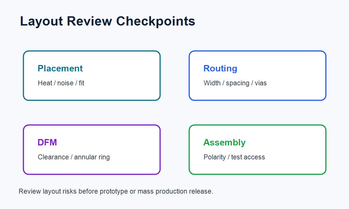
For production orders, DFM review should happen before the buyer locks the design. For prototypes, it is still important because a prototype built with risky geometry may produce misleading test results or delay the next revision.
Assembly-Friendly Layout Reduces Placement and Soldering Defects
PCB layout also controls how easy the board is to assemble. Design for assembly focuses on component spacing, footprint accuracy, orientation, solder paste openings, fiducials, test points, rework access, and inspection visibility.
- Use verified footprints for the exact component package.
- Keep polarity marks clear for ICs, diodes, LEDs, electrolytic capacitors, and connectors.
- Provide fiducials when the assembly process requires them.
- Avoid placing tall components where they block inspection or rework.
- Keep test points accessible for programming, power, ground, and important signals.
- Review double-sided assembly risk when heavy or heat-sensitive parts are involved.
Common PCB Layout Mistakes Can Delay Prototype and Production
Many layout mistakes are found only after quotation, DFM review, assembly setup, or first-article inspection. Catching them before file release saves time and reduces rework.
| Mistake | Possible Result | Prevention |
| Wrong footprint | Component cannot be assembled or soldered correctly | Match footprint to the manufacturer datasheet and sample package. |
| Insufficient clearance | Fabrication rejection, solder bridge, or safety concern | Use factory design rules and product voltage requirements. |
| Poor return path | Noise, EMI, unstable signals, or reset problems | Plan ground reference and current loops before routing. |
| Missing test access | Hard debug and slow production testing | Add accessible test points for key nets and programming. |
| Incomplete output package | Quotation delay or production questions | Send Gerber or ODB++, drill, BOM, CPL, stackup, and notes together. |
PCB Layout Cost Depends on Density, Layers, and Process Limits
The layout itself influences the final PCB cost because it determines layer count, material needs, copper weight, trace and spacing limits, drill size, via type, controlled impedance, surface finish, assembly complexity, and testing requirements.
- More layers: increase fabrication complexity but can improve routing, grounding, and performance.
- Tighter geometry: smaller traces, spaces, and holes require stronger process control.
- Advanced vias: blind vias, buried vias, microvias, and via-in-pad raise cost and inspection needs.
- Dense assembly: BGAs, fine-pitch ICs, and double-sided SMT require careful DFA review.
- Testing: flying probe, functional testing, programming, or fixtures add value but also affect quotation.
A Supplier Should Review Layout Risks Before Production
A reliable PCB/PCBA supplier should not simply accept files without review when the design has manufacturing or assembly risk. For prototype, OEM, ODM, and mass production projects, early communication between the buyer, layout engineer, and factory helps prevent avoidable delays.
- Ask whether the supplier can review DFM and DFA issues before fabrication.
- Confirm minimum trace, spacing, drill, annular ring, copper, and solder mask limits.
- Ask how stackup, controlled impedance, and material questions are handled.
- Confirm whether PCB fabrication, component sourcing, assembly, inspection, and testing can be coordinated.
- Ask what inspection evidence is available for prototypes and production builds.
Use This PCB Layout Release Checklist
Before sending a PCB layout for quotation or production, check that the file package is complete and the design has been reviewed for manufacturing, assembly, and testing.
- Confirm schematic and layout netlist match.
- Run electrical rule checks and design rule checks.
- Check board outline, mounting holes, keep-outs, and connector positions.
- Verify trace width, spacing, drill size, annular ring, and copper clearance.
- Confirm stackup, finished thickness, copper weight, and material requirements.
- Review polarity, pin 1 marks, component orientation, and assembly notes.
- Export Gerber or ODB++, drill files, BOM, CPL, and drawings from the same revision.
- Define testing requirements before production starts.
- Keep revision numbers clear in file names and quotation communication.
Frequently Asked Questions About PCB Layout
What is PCB layout?
PCB layout is the process of turning a circuit schematic into a physical printed circuit board design with component placement, copper routing, vias, layers, board outline, and manufacturing output files.
Is PCB layout the same as PCB design?
PCB layout is one part of PCB design. PCB design includes the circuit idea, schematic, component selection, simulation when needed, layout, DFM review, output files, prototype testing, and revisions.
What files come from PCB layout?
Common layout outputs include Gerber or ODB++ files, drill files, netlist, BOM, CPL or pick-and-place file, assembly drawing, fabrication notes, and sometimes impedance or stackup documents.
Why is PCB layout important?
PCB layout affects signal integrity, power delivery, heat dissipation, mechanical fit, assembly yield, inspection access, testing, reliability, cost, and production lead time.
What is routing in PCB layout?
Routing is the process of connecting component pads with copper traces and vias according to the schematic netlist while meeting electrical and manufacturing constraints.
What is component placement in PCB layout?
Component placement decides where each part sits on the board. Good placement keeps critical paths short, supports routing, controls heat, fits the enclosure, and improves assembly quality.
What is DFM in PCB layout?
DFM means design for manufacturability. In PCB layout, it checks whether trace width, spacing, drill size, annular ring, solder mask, copper clearance, and panel needs can be manufactured reliably.
What makes PCB layout expensive?
Cost can increase with more layers, tighter trace spacing, smaller holes, controlled impedance, special materials, blind or buried vias, via-in-pad, dense BGAs, double-sided assembly, and extra testing.
How do I know if a PCB layout is good?
A good PCB layout matches the schematic, passes design rule checks, supports assembly and testing, follows manufacturing limits, controls noise and heat, and has complete output files.
Can a manufacturer fix PCB layout problems?
A manufacturer can flag DFM and assembly risks, but major layout problems usually need to be corrected in the design files before fabrication or assembly.
When should PCB layout be reviewed?
Review PCB layout before prototype release, after major component substitutions, before panelization, and before moving from prototype to mass production.
What should buyers send for PCB layout-based quotations?
Buyers should send Gerber or ODB++ files, drill files, BOM, CPL for assembly, stackup or material requirements, surface finish, quantity, testing needs, and any special quality requirements.
Final Takeaway
PCB layout is where electrical design becomes a real product-ready board. Good layout balances placement, routing, stackup, manufacturability, assembly, testing, cost, and reliability instead of treating the board as only a wiring exercise.
If you’re sourcing reliable PCB/PCBA manufacturing, including OEM, ODM, prototyping, mass production, or custom engineering solutions, reach out to our engineering team for technical support and a quote at [email protected].



0 Comments